Composition for forming organic insulating film and organic insulating film formed from the same

a technology of organic insulating film and organic insulating film, which is applied in the direction of thermoelectric device junction material, solid-state device, electrical apparatus, etc., can solve the problems of inability to replace inorganic insulating film, inability to meet the requirements of plastic substrates, and inability to meet the requirements of organic solvents, etc., to achieve excellent chemical resistance to organic solvents and improve the electrical performance of transistors

Active Publication Date: 2007-08-14
SAMSUNG ELECTRONICS CO LTD
View PDF9 Cites 5 Cited by
  • Summary
  • Abstract
  • Description
  • Claims
  • Application Information

AI Technical Summary

Benefits of technology

[0009]Therefore, the present invention has been made in view of the above problems, and it is a feature of the present invention to provide an organic insulating film having excellent chemical resistance to organic solvents used in a subsequent photolithographic process. Accordingly, when the organic insulating film is used to fabricate a transistor, it can improve the electrical performance of the transistor while enabling the formation of micropatterns.

Problems solved by technology

However, these inorganic oxide materials do not have any advantages over conventional silicon materials in terms of processing.
However, since these organic insulating films exhibit unsatisfactory device characteristics over inorganic insulating films, they are unsuitable to replace inorganic insulating films.
However, there still remains a problem that the organic insulating polymer may be dissolved in an organic solvent used in a subsequent photolithographic process.
However, this attempt is limited in its application to plastic substrates since a high temperature of about 200° C. is required to crosslink PVP (Journal of Applied Physics 2003, 93, 2977 & Applied Physics Letter 2002, 81, 289).

Method used


Image

  • Composition for forming organic insulating film and organic insulating film formed from the same
  • Composition for forming organic insulating film and organic insulating film formed from the same
  • Composition for forming organic insulating film and organic insulating film formed from the same

Examples


example 2

PREPARATIVE EXAMPLE 2

Preparation of Coating Solution for Formation of Organic Insulating Film

[0092]7 g of the organic insulating polymer prepared in Preparative Example 1, 1.5 g of poly(ethylene-co-methyl acrylate-co-glycidyl methacrylate) of Formula 21a below (Aldrich) as a crosslinking agent, 1.5 g of poly(ethylene-co-methyl acrylic acid) of Formula 21b below (Aldrich) as another crosslinking agent, and 0.1 g of a photoacid generator of Formula 22 below (PAC200, Miwon Commercial Co. Ltd., Korea) were dissolved in a mixed solution of 73 g of cyclohexanone and 4.5 g of diethylene glycol methyl ethyl ether to prepare a coating solution for the formation of an organic insulating film.

[0093]

example 1

Fabrication of Organic Thin Film Transistor

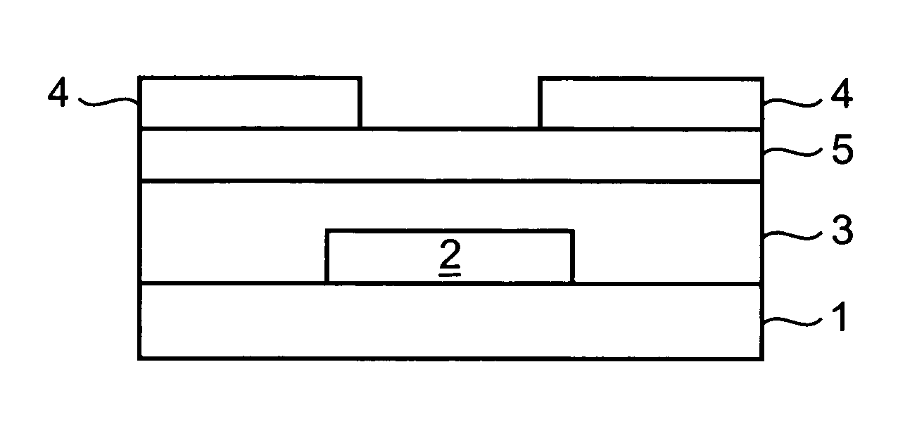
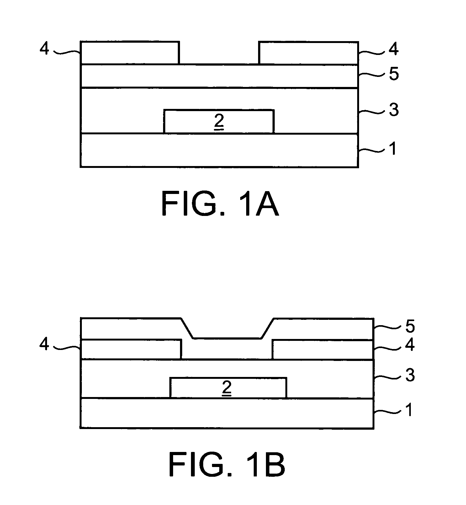
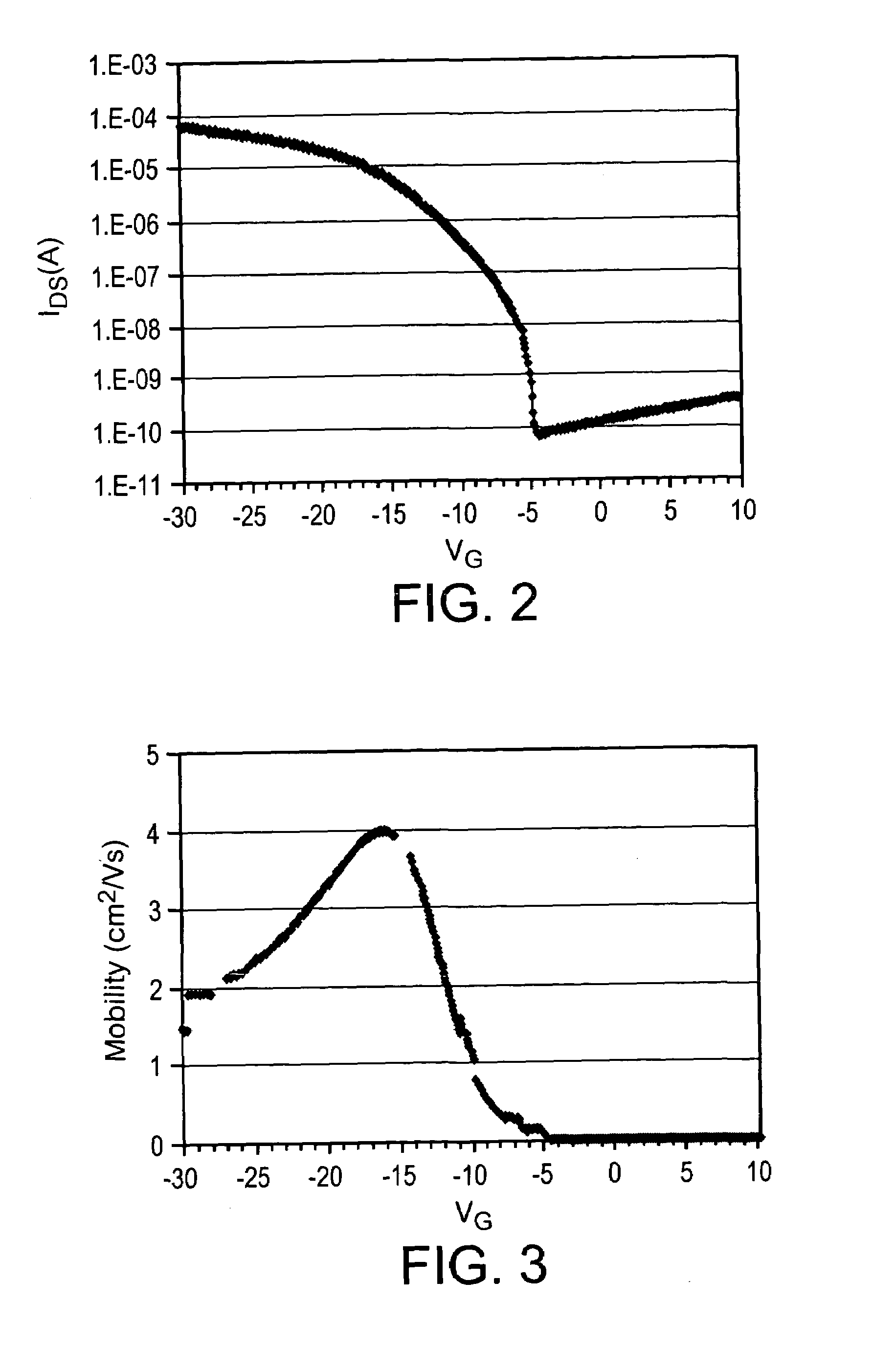
[0094]In this example, a bottom-contact organic thin film transistor was fabricated (FIG. 1b). First, Al was deposited on a washed glass as a substrate by a vacuum deposition technique to form a gate electrode having a thickness of 1,500 Å. The coating solution for forming an organic gate insulating film, which was prepared in Preparative Example 2, was coated onto the gate electrode to a thickness of 5,000 Å by spin coating at 4,000 rpm, prebaked at 100° C. for 3 minutes, irradiated by 600 W UV for 20 seconds, and baked at 100° C. for 1 hour to form an organic insulating film. Next, Au was deposited on the organic gate insulating film to a thickness of 1,000 Å, and was subjected to a photographic process to form an Au electrode pattern. Pentacene was deposited on the Au electrode pattern to a thickness of 1,000 Å by organic molecular beam deposition (OMBD) under a vacuum of 2×10⁻⁷ torr, a substrate temperature of 50° C. and a deposition ra...


PUM

PropertyMeasurementUnit
temperatureaaaaaaaaaa
compositionaaaaaaaaaa
insulatingaaaaaaaaaa

Abstract

Disclosed herein is a composition for forming an organic insulating film and an organic insulating film formed from the composition. An exemplary composition comprises an insulating polymer having a maleimide structure, a crosslinking agent and a photoacid generator so as to form a crosslinked structure. The organic insulating film has excellent chemical resistance to organic solvents used in a subsequent photolithographic process and can improve the electrical properties of transistors.

Description

BACKGROUND OF THE INVENTION[0001]This non-provisional application claims priority under 35 U.S.C. § 119(a) to Korean Patent Application No. 2003-90309 filed on Dec. 11, 2003, which is herein incorporated by reference.FIELD OF THE INVENTION[0002]The present invention relates to a composition for forming an organic insulating film, and an organic insulating film formed from the composition. More particularly, the present invention relates to a composition for forming an organic insulating film crosslinked so as to have excellent chemical resistance to organic solvents used in a photolithographic process after formation of the organic insulating film, and an organic insulating film formed from the composition.DESCRIPTION OF THE RELATED ART[0003]Since polyacetylenes as conjugated organic polymers exhibiting semiconductor characteristics were developed, organic semiconductors have been actively investigated as novel electrical and electronic materials in a wide variety of applications, e...

Claims


Application Information

Patent Timeline
Patent Type & Authority Patents(United States)
IPC IPC(8): C07D207/444C08L35/00C08G61/12C08G73/06C08K5/00C08L79/04C08L101/00C09D159/00G03F7/004G03F7/038H01B3/44H01L21/312H01L35/24H01L51/05
CPCC08G61/124C08G73/0611C08L79/04C09D159/00G03F7/0045G03F7/0382H01B3/442H01L21/312H01L51/052H01L21/02118H10K10/471C08G73/06H01L21/02348
Inventor JEONG, EUN JEONGKOO, BON WONKIM, JOO YOUNGKANG, IN NAM
Owner SAMSUNG ELECTRONICS CO LTD
Why Eureka
Try Eureka