Semiconductor device

a technology of semiconductor devices and insulating films, applied in semiconductor devices, semiconductor/solid-state device details, electrical devices, etc., can solve the problems of low mechanical strength of porous insulating films, low mechanical strength and low adhesion of interlayer insulating films

Active Publication Date: 2007-08-21
KIOXIA CORP
View PDF6 Cites 56 Cited by
  • Summary
  • Abstract
  • Description
  • Claims
  • Application Information

AI Technical Summary

Problems solved by technology

Unfortunately, these porous insulating films generally have low mechanical strength.
The low mechanical strength and low adhesion of an interlayer insulating film pose problems such as film peeling in steps in which heating is performed.

Method used


Image

  • Semiconductor device
  • Semiconductor device
  • Semiconductor device

Examples


first embodiment

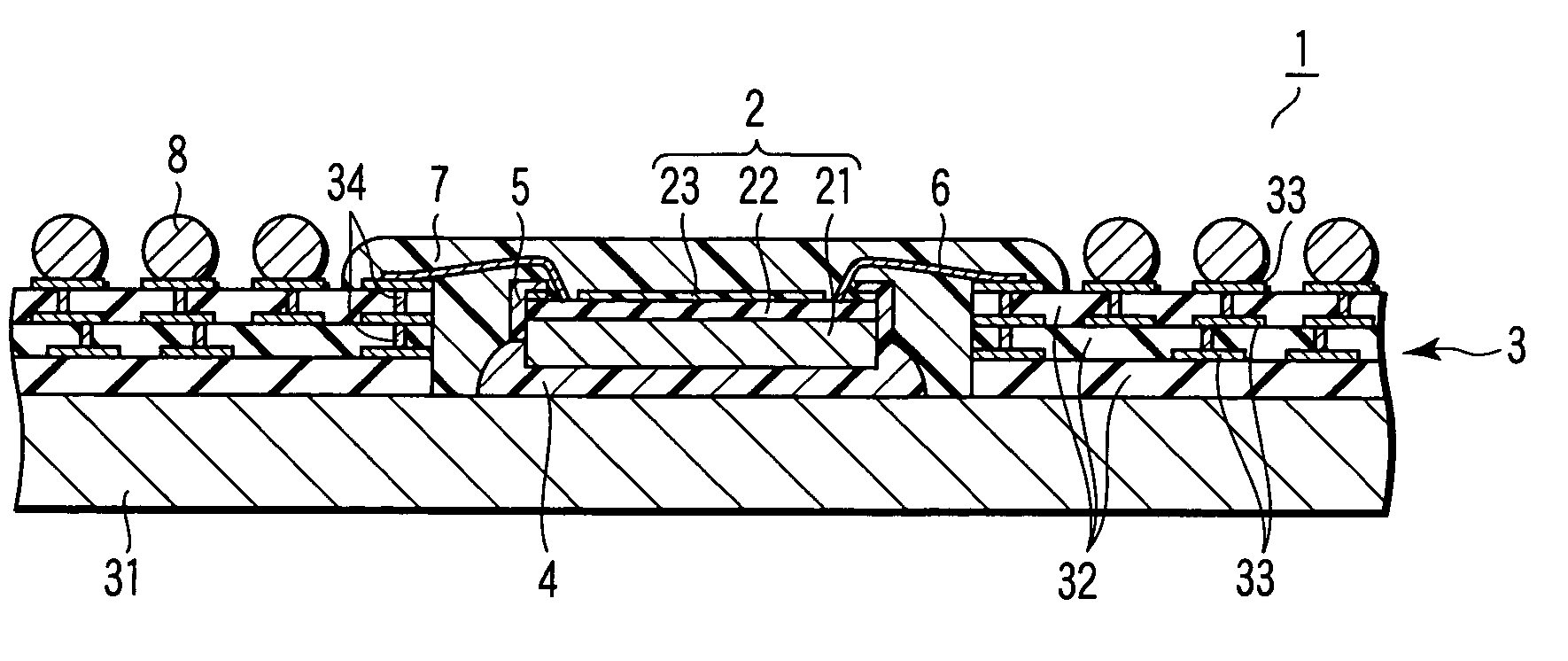
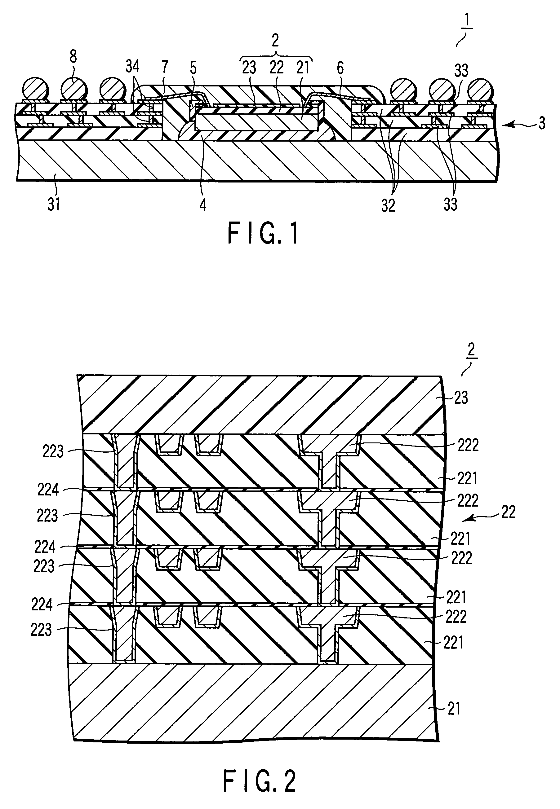
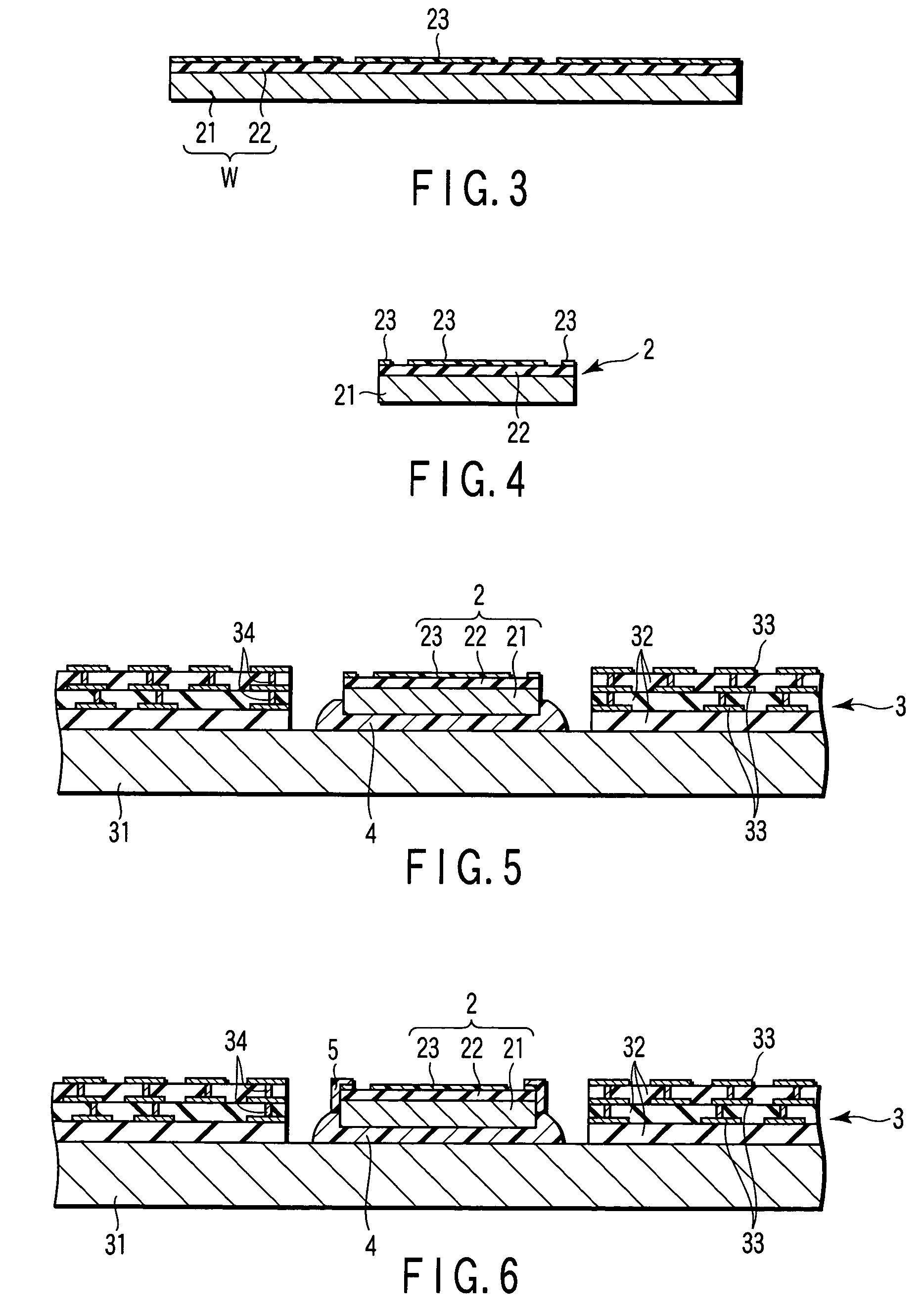
[0022]FIG. 1 is a sectional view schematically showing a semiconductor device according to the present invention. FIG. 2 is a sectional view schematically showing an example of a semiconductor chip usable in the semiconductor device shown in FIG. 1.

[0023]The semiconductor device 1 shown in FIG. 1 is a semiconductor package called an enhanced ball grid array (EBGA). The semiconductor package 1 includes a semiconductor chip 2, a wiring substrate 3, a mounting material 4, a stress relaxing resin layer 5, bonding wires 6, a resin encapsulating layer 7, and metal bumps 8.

[0024]The semiconductor chip 2 includes a semiconductor substrate 21 such as a silicon substrate. Various elements such as transistors are formed on one major surface of the semiconductor substrate 21.

[0025]A multilayer interconnection structure 22 is formed on this major surface of the semiconductor substrate 21. The multilayer interconnection structure 22 includes a plurality of interlayer insulating films 221 and a pl...

second embodiment

[0052]the present invention will be described below.

[0053]FIG. 9 is a sectional view schematically showing a semiconductor device according to the second embodiment of the present invention. A semiconductor device 1 has the same structure as the semiconductor package 1 according to the first embodiment except that a stress relaxing resin layer 5 covers the edges of a semiconductor chip 2 on the side of a multilayer interconnection structure 22 and covers a central portion of the major surface of the semiconductor chip 2 on the side of the multilayer interconnection structure 22. When this structure is used, the same effects as explained in the first embodiment can be obtained.

[0054]Also, in the semiconductor package 1 shown in FIG. 9, the stress relaxing resin layer 5 covers the central portion of the major surface of the semiconductor chip 2 on the side of the multilayer interconnection structure 22. When this structure is used, a larger amount of material is necessary to form the ...

third embodiment

[0055]the present invention will be described below.

[0056]FIG. 10 is a sectional view schematically showing a semiconductor device according to the third embodiment of the present invention. A semiconductor device 1 has the same structure as the semiconductor package 1 according to the first embodiment except that the buffer coating layer 23 is omitted. When this structure is used, almost the same effects as explained in the first embodiment can be obtained.

[0057]Since the buffer coating layer 23 is omitted from the semiconductor package 1 shown in FIG. 10, a stress larger than that in the semiconductor package 1 of the first embodiment acts on a central portion of the major surface of the semiconductor chip 2 on the side of the multilayer interconnection structure 22. However, the semiconductor package 1 shown in FIG. 10 is more advantageous in reducing the fabrication cost than the semiconductor package 1 of the first embodiment.


PUM


Abstract

There is provided a semiconductor device including a semiconductor chip which includes a semiconductor substrate and a multilayer interconnection structure formed thereon, the multilayer interconnection structure including an interlayer insulating film smaller in relative dielectric constant than an SiO2 film, an encapsulating resin layer which covers a major surface of the semiconductor chip on a side of the multilayer interconnection structure and covers a side surface of the semiconductor chip, and a stress relaxing resin layer which is interposed between the semiconductor chip and the encapsulating resin layer, covers at least a part of an edge of the semiconductor chip on the side of the multilayer interconnection structure, and is smaller in Young's modulus than the encapsulating resin layer.

Description

CROSS-REFERENCE TO RELATED APPLICATIONS[0001]This application is based upon and claims the benefit of priority from prior Japanese Patent Application No. 2004-066113, filed Mar. 9, 2004, the entire contents of which are incorporated herein by reference.BACKGROUND OF THE INVENTION[0002]1. Field of the Invention[0003]The present invention relates to a semiconductor device and, more particularly, to a semiconductor device having a structure in which a semiconductor chip is covered with an encapsulating resin layer.[0004]2. Description of the Related Art[0005]Semiconductor devices such as a large-scale integrated circuit (LSI) are required to have high speed. To meet this requirement, it is recently being attempted to use low-resistivity materials as wires and decrease the relative dielectric constant of an interlayer insulating film. More specifically, the wiring material is being changed from Al to Cu. Also, as an interlayer insulating film, it is being considered to use a so-called “...

Claims


Application Information

Patent Timeline
Patent Type & Authority Patents(United States)
IPC IPC(8): H01L23/12H01L23/28H01L23/29H01L21/00H01L21/56H01L21/768H01L23/31H01L29/40
CPCH01L23/13H01L23/3121H01L23/3185H01L23/49816H01L23/562H01L2224/32225H01L2224/48227H01L2224/73265H01L2924/15321H01L2224/32245H01L2924/00012H01L24/73H01L2924/14H01L2224/92247H01L2924/15153H01L2924/181H01L2924/00
Inventor SETO, MASAHARU
Owner KIOXIA CORP
Why Eureka
Try Eureka