
Tunable wideband bandpass filter, tunable multi-band bandpass filter using the same, and methods therefore

a wideband bandpass filter and multi-bandbandpass technology, applied in waveguide devices, electrical equipment, resonance circuit tuning, etc., can solve the problems of frequency-tunable bandpass, severe non-linear characteristics, multi-band and multi-mode receivers that require additional receivers and space, etc., and achieve low power consumption

Active Publication Date: 2007-08-21
SAMSUNG ELECTRONICS CO LTD
View PDF3 Cites 50 Cited by
  • Summary
  • Abstract
  • Description
  • Claims
  • Application Information

AI Technical Summary

Benefits of technology

The invention provides a small-sized, low power-consuming tunable wideband bandpass filter that can vary the center frequency and bandwidth of a signal to be filtered. The filter includes a plurality of switched-capacitor banks and a plurality of inductors integrated into a single chip. The switched-capacitor banks include a plurality of switched capacitors and switching elements, which can be metal oxide semiconductor transistors or micro electro mechanical system switches. The filter can be controlled by a digital signal and can be used in a tunable multi-band wideband bandpass filter. The technical effects of the invention include a compact size, low power consumption, and wide bandwidth coverage.

Problems solved by technology

Thus, the multi-band and multi-mode receiver requires additional receivers and space.
However, the conventional frequency-tunable bandpass filter described above has severe non-linear characteristics, a large size, increased power consumption, and is costly.
On the other hand, a frequency-tunable RF bandpass filter using only active elements is easily controlled; however, it consumes a lot of power, has a low yield, and performs worse than the passive filter in terms of linearity or noise factor.
As such, the frequency-tunable bandpass filter using only active elements is difficult to apply to the wideband communication systems or multi-mode communication systems.

Method used


Image

  • Tunable wideband bandpass filter, tunable multi-band bandpass filter using the same, and methods therefore
  • Tunable wideband bandpass filter, tunable multi-band bandpass filter using the same, and methods therefore
  • Tunable wideband bandpass filter, tunable multi-band bandpass filter using the same, and methods therefore

Examples


Embodiment Construction

[0044]Reference will now be made in detail to the embodiments of the present invention, examples of which are illustrated in the accompanying drawings, wherein like reference numerals refer to the like elements throughout. The embodiments are described below to explain the present invention by referring to the figures.

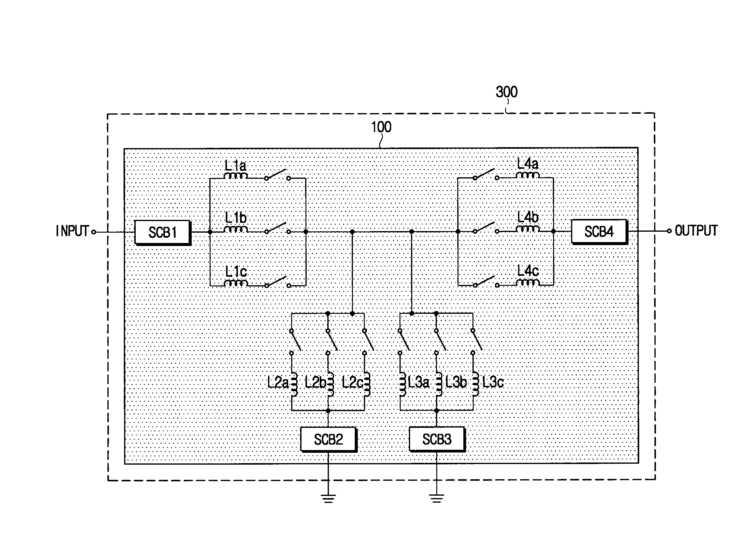
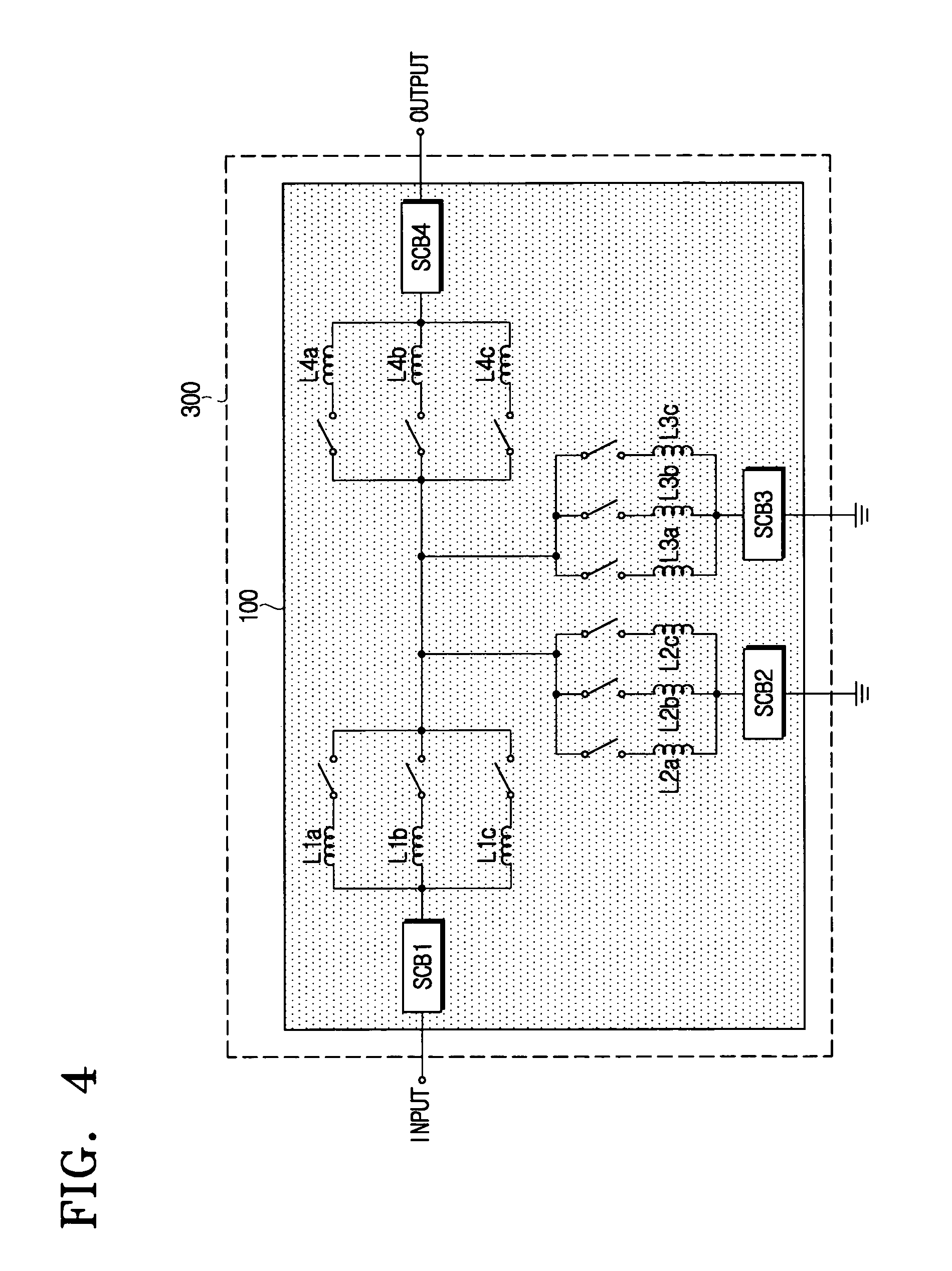
[0045]FIG. 4 is an illustration of a structure of a tunable multi-band wideband bandpass filter according to an embodiment of the invention. In FIG. 4, a tunable multi-band wideband bandpass filter 300 has a plurality of switched-capacitor banks (“SCB”) SCB1, SCB2, SCB3, and SCB4 and a plurality of switched-inductor banks (L1a, L1b, and L1c), (L2a, L2b, and L2c), (L3a, L3b, and L3c), and (L4a, L4b, and L4c), respectively integrated on a side of a CMOS chip 100. For example, the plurality of SCBs and switched-inductor banks are provided on an upper side of the CMOS chip 100. The capacitors and inductors are switched in order to improve the performance of the filter by e...


PUM


Abstract

A tunable wideband bandpass filter that can digitally vary the center frequency and bandwidth of a signal to be filtered, and includes a plurality of switched-capacitor banks for varying capacitance and converting the center frequency and bandwidth into a digital signal, and a plurality of inductors provided for inductance to generate the center frequency, the plurality of switched-capacitor banks that may be integrated into a signal chip.

Description

CROSS-REFERENCE TO RELATED APPLICATION[0001]This application claims benefit under 35 U.S.C. § 119 from Korean Patent Application No. 2004-11670, filed on Feb. 21, 2004, the content of which is incorporated herein by reference.BACKGROUND OF THE INVENTION[0002]1. Field of the Invention[0003]The present invention relates to a frequency-tunable filter, and more particularly to digitally-controlled, small-sized, low power-consuming tunable wideband filter and tunable multi-band wideband filter using switched capacitors and inductors in use of the same, which are suitable for wideband communication systems and multi-mode communication systems.[0004]2. Description of the Related Art[0005]In general, frequency-tunable bandpass filters with freely variable center frequencies are required in wideband communication systems, such as television (“TV”), ultra highband (“UWB”), and multi-mode communication systems, such as cellular phones, personal communication service (“PCS”), and wideband code-...

Claims


Application Information

Patent Timeline
Patent Type & Authority Patents(United States)
IPC IPC(8): H03H7/00H03H7/01H01P1/20H03H7/12
CPCH03H7/0115H03H7/0161H03H7/1766H03H7/1775H03H2210/025H03H2210/015H03H2210/021H03J2200/10H03H2210/012H03H7/175H03H7/1758H01P1/20
Inventor SON, MI-HYUNLEE, SEONG-SOOLEE, KWY-ROLEE, MIN-KYUNGKWON, ICK-JIN
Owner SAMSUNG ELECTRONICS CO LTD
Learn More