3D interconnect with protruding contacts

a technology of protruding contacts and interconnects, which is applied in the direction of semiconductor devices, semiconductor/solid-state device details, electrical apparatus, etc., can solve the problems of difficult planarization of interconnects, interconnect between two substrates may fail, and plasma-enhanced bonding may fail, etc., to achieve excellent electrical contact characteristics, good durability, and easy assembly

Active Publication Date: 2007-08-28
HEWLETT-PACKARD ENTERPRISE DEV LP +1
View PDF23 Cites 396 Cited by
  • Summary
  • Abstract
  • Description
  • Claims
  • Application Information

AI Technical Summary

Benefits of technology

[0013]The preferred semiconductor, according to various embodiments of the present invention, offers the following advantages: ease of assembly; excellent electrical contact characteristics; and good durability. In fact, in many of the preferred embodiments, these factors of ease of assembly and excellent electrical contact characteristics are optimized to an extent that is considerably higher than heretofore achieved in prior, known semiconductor devices.

Problems solved by technology

It is well known that the CMP planarization process creates some unique challenges for wafer-to-wafer interconnect applications since it is difficult to planarize the interconnect plug (or contact points) and the surrounding area evenly.
The interconnect between two substrates may fail if dishing on the plugs occurs during the CMP process.
Also, plasma-enhanced bonding may fail if the plugs surfaces are higher than the surrounding area, which prevents the two substrates from contacting at the atomic level.
This approach works fine for many 3-D interconnect applications, but does not work when both 3-D interconnect and hermetic packaging are required since BCB is not hermetic.
However, none of these techniques provide both a good electrical interconnect between the substrates and hermetic packaging at the wafer level as the bumps or balls tend to cause a standoff between the circuits or substrates.
The interconnect density is also limited with this approach.
However, many of these techniques do not provide an adequate bond for a variety of reasons.

Method used


Image

  • 3D interconnect with protruding contacts
  • 3D interconnect with protruding contacts
  • 3D interconnect with protruding contacts

Examples


Embodiment Construction

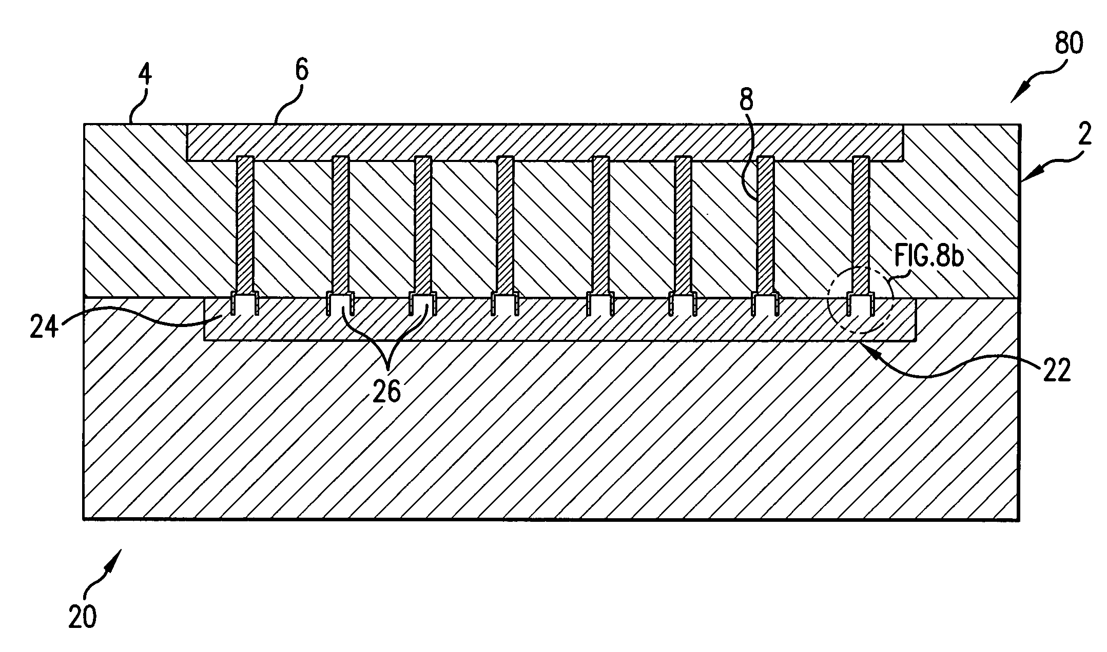
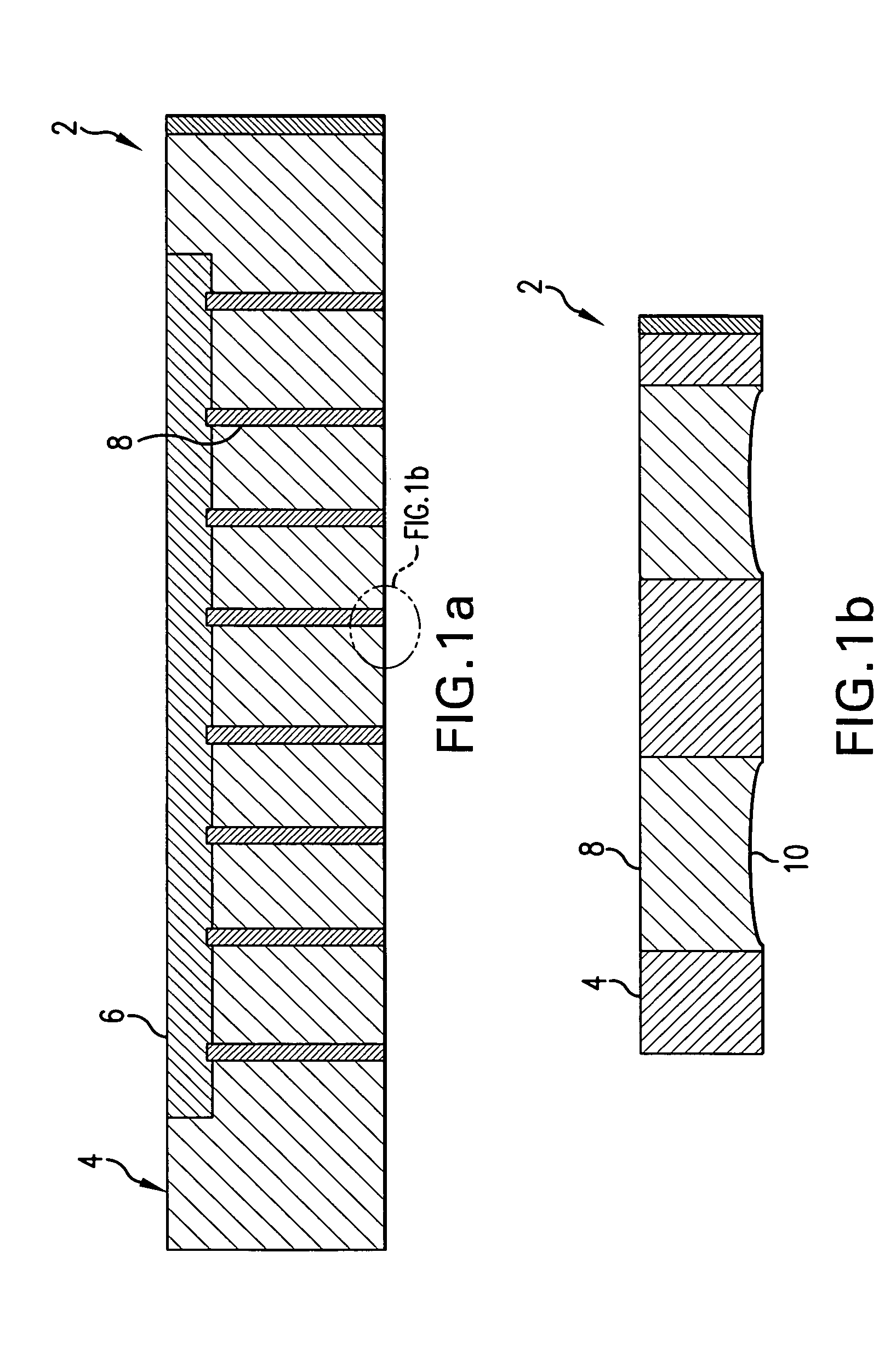
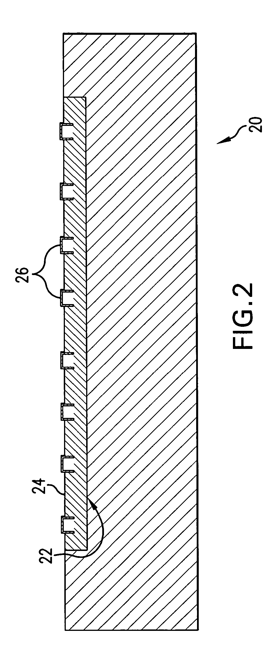
[0025]With reference first to FIG. 1, there is illustrated one preferred embodiment for use of the concepts of this invention. FIG. 1 illustrates a first semiconductor substrate 2. Substrate 2 includes, in part, complementary metal oxide semiconductor (CMOS) 6, and through silicon interconnect plugs 8. Preferably, substrate 2 may be conventionally thinned and chemically mechanically polished (CMP) on the backside to prepare the plugs 8 for bonding. Also, through silicon interconnect plugs can be constructed of any suitable material such as tungsten, copper, gold or the like. Finally, each substrate 2 and 20 (FIG. 2) may not contain through silicon interconnect plugs 8 and the two substrates can be bonded together face-to-face.

[0026]With respect to FIG. 1b, a detailed view of the dished surface 10 of the through silicon interconnect plug 8 is illustrated. The dished surface 10 typically results from the CMP process. It is to understood that the dished surface 10 that opposes the prot...


PUM


Abstract

This invention relates to a semiconductor having protruding contacts comprising, a first semiconductor substrate having at least one interconnect located substantially within the first substrate, and a second semiconductor substrate having at least one protruding contact point that substantially contacts at least one interconnect.

Description

BACKGROUND OF THE INVENTION[0001]1. Field of the Invention[0002]This invention relates to a semiconductor having protruding contacts comprising, a first semiconductor substrate having at least one interconnect located substantially within the first substrate, and a second semiconductor substrate having at least one protruding contact point that substantially contacts at least one interconnect.[0003]2. Description of the Related Art[0004]Prior to the present invention, as set forth in general terms above and more specifically below, it is known in the semiconductor art, that two semiconductor substrates can be joined together at low temperatures by using well-known plasma-enhanced bonding processes. These low-temperature substrate joining techniques can be used to package MEMS (microelectromechanical systems) or NEMS (nanoelectromachanical systems) devices hermetically as well as 3-D wafer stacking. With respect to these low-temperature substrate joining techniques, the surface of th...

Claims


Application Information

Patent Timeline
Patent Type & Authority Patents(United States)
IPC IPC(8): H01L23/48
CPCH01L21/76898H01L23/481H01L24/03H01L24/05H01L24/72H01L24/80H01L25/0657H01L2924/1461H01L2224/0401H01L2924/01033H01L2924/01005H01L2924/1433H01L2924/14H01L2924/014H01L2224/05644H01L2224/05647H01L2224/05655H01L2224/13144H01L2225/06513H01L2225/06541H01L2924/01014H01L2924/01018H01L2924/01029H01L2924/01074H01L2924/01079H01L2924/01322H01L2924/00014H01L2924/00H01L2924/15788
Inventor CHEN, CHIEN-HUACHEN, ZHIZHANGMEYER, NEAL W.
Owner HEWLETT-PACKARD ENTERPRISE DEV LP
Why Eureka
Try Eureka