Laser beam processing method for a semiconductor wafer

a technology of laser beam and semiconductor wafer, which is applied in the direction of semiconductor/solid-state device details, manufacturing tools, crystal growth process, etc., can solve the problems of deteriorating semiconductor chips, affecting the processing efficiency of semiconductor chips, so as to achieve smooth removal of low-k films

Active Publication Date: 2007-09-04
DISCO CORP
View PDF20 Cites 136 Cited by
  • Summary
  • Abstract
  • Description
  • Claims
  • Application Information

AI Technical Summary

Benefits of technology

[0006]It is an object of the present invention to provide a laser beam processing method and a laser beam processing machine which are capable of smoothly removing a Low-k film formed on streets formed on a semiconductor substrate and metal patterns for testing partially formed on each street.

Problems solved by technology

As the Low-k film is a laminate consisting of multiple layers (5 to 15 layers) like mica and extremely fragile, when the semiconductor wafer is cut along a street with the cutting blade, the Low-k film is peeled off, and this peeling reaches a circuit and gives a fatal blow to a semiconductor chip.
However, in a semiconductor wafer having metal patterns for testing called “test element group (Teg)” for testing the function of each circuit partially formed on the Low-k film on the streets, it involves a problem that even when a laser beam is applied to remove the Low-k film, the metal patterns made of copper or aluminum interfere the laser beam, thereby making it impossible to remove the Low-k film smoothly.
As a countermeasure, when a laser beam is applied to the streets upon increasing the output of the laser beam to such an extent that the metal patterns can be removed, a new problem arises that the semiconductor substrate of a street portion where only the Low-k film is formed is broken and debris is scattered and adhered to a bonding pad connected to the circuit, thereby deteriorating the semiconductor chips.

Method used


Image

  • Laser beam processing method for a semiconductor wafer
  • Laser beam processing method for a semiconductor wafer
  • Laser beam processing method for a semiconductor wafer

Examples


Embodiment Construction

[0026]The laser beam processing method and laser beam processing machine according to the present invention will be described in detail hereinunder with reference to the accompanying drawings.

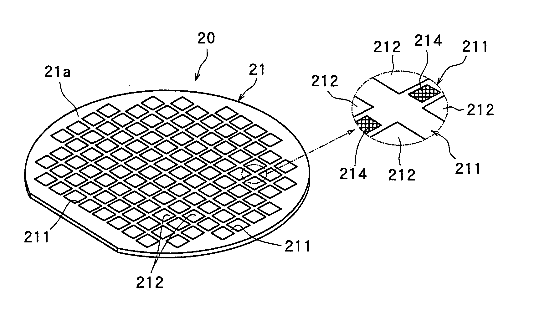
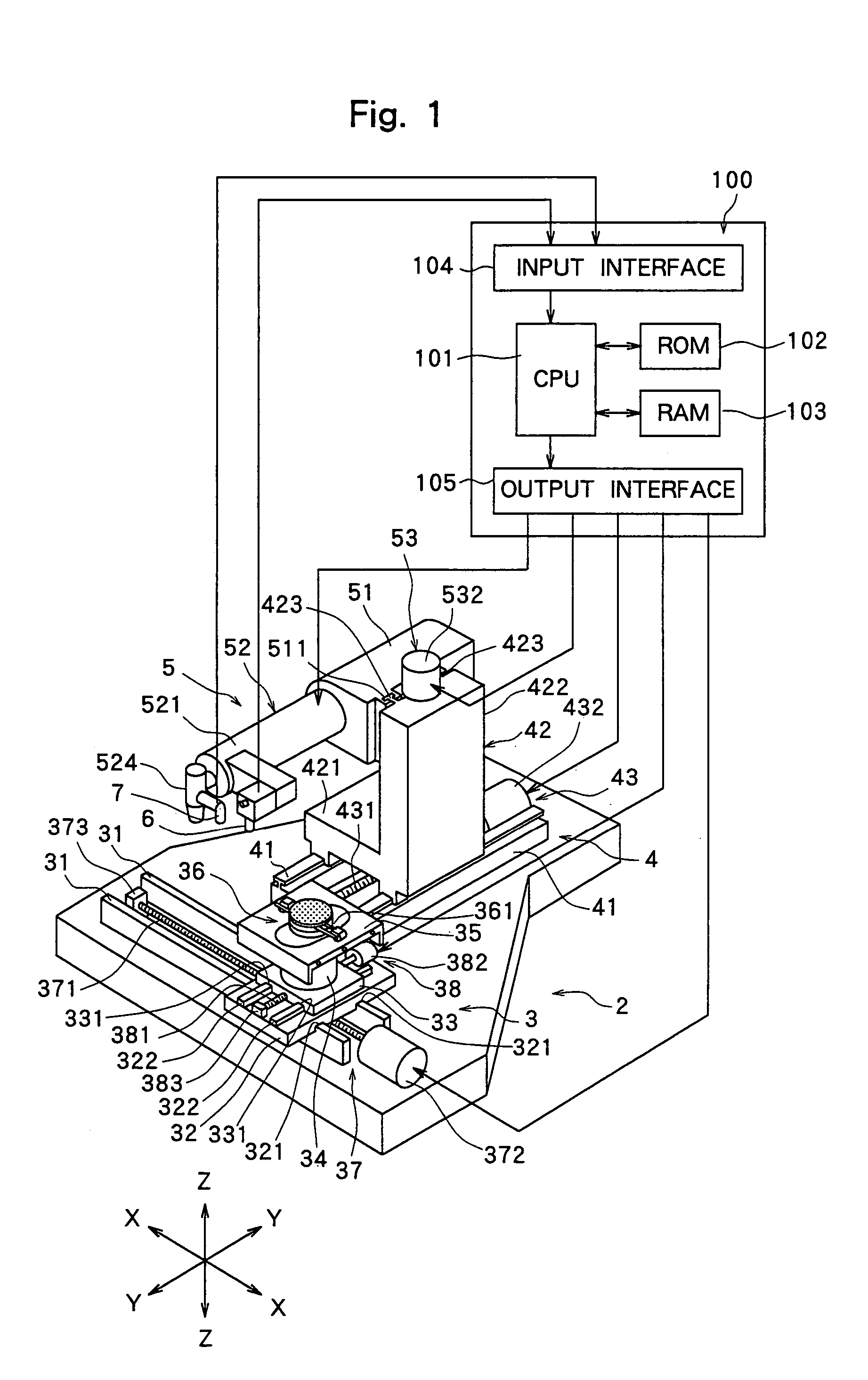
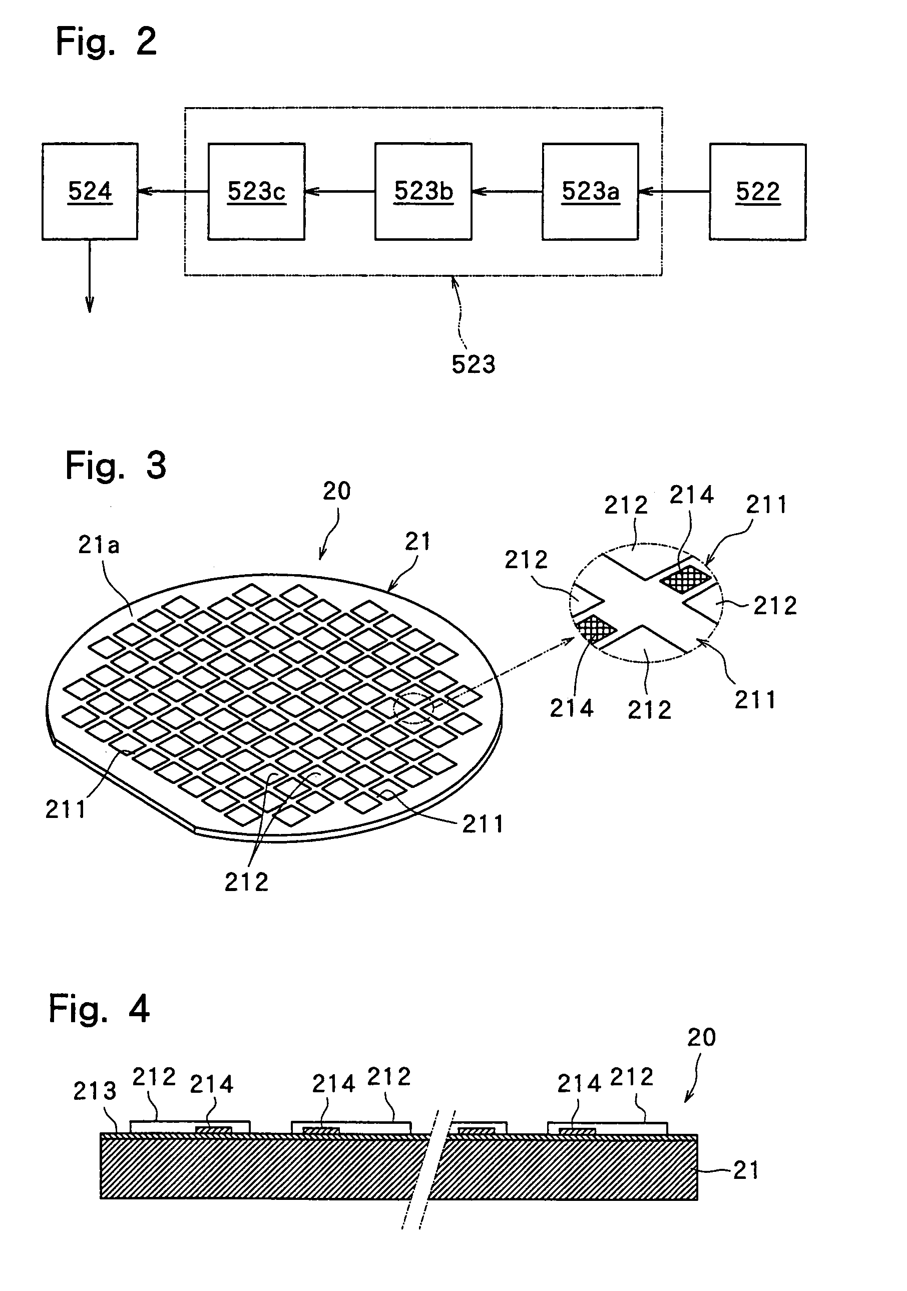
[0027]FIG. 1 is a perspective view of a laser beam processing machine constituted according to the present invention. The laser beam processing machine 1 shown in FIG. 1 comprises a stationary base 2, a chuck table mechanism 3 that is disposed on the stationary base 2 in such a manner that it can move in a direction indicated by an arrow X and holds a workpiece, a laser beam application unit support mechanism 4 disposed on the stationary base 2 in such a manner that it can move in a direction indicated by an arrow Y perpendicular to the direction indicated by the arrow X, and a laser beam application unit 5 disposed on the laser beam application unit support mechanism 4 in such a manner that it can move in a direction indicated by an arrow Z.

[0028]The above chuck table mechanism 3 comprises a p...


PUM

PropertyMeasurementUnit
diameteraaaaaaaaaa
thickaaaaaaaaaa
dielectricaaaaaaaaaa

Abstract

A laser beam processing method for a semiconductor wafer having a low-dielectric insulating film formed on the front surface of a semiconductor substrate thereof, a plurality of circuits sectioned by streets into a lattice pattern, and metal patterns for testing formed partially on each street. The method includes a laser beam processing step for applying a laser beam to the positions of areas at which the metal patterns are located, and to the low-dielectric insulating film, under different processing conditions so as to remove the metal patterns and the low-dielectric insulating film without damaging the substrate and its circuits.

Description

FIELD OF THE INVENTION[0001]The present invention relates to a laser beam processing method for a semiconductor wafer which has a low-dielectric insulating film formed on the front surface, a plurality of circuits formed by streets formed in a lattice pattern and metal patterns for testing partially formed on each street, and to a laser beam processing machine.DESCRIPTION OF THE PRIOR ART[0002]As is known to people of ordinary skill in the art, in the production process of a semiconductor device, a semiconductor wafer having a plurality of areas sectioned by streets (cutting lines) formed in a lattice pattern on the front surface of a substantially disk-like semiconductor substrate and circuits such as IC's or LSI's formed in the sectioned areas is cut along the streets to be divided into individual semiconductor chips. Cutting along the streets of the semiconductor wafer is generally carried out by a cutting machine called “dicer”. This cutting machine comprises a chuck table for h...

Claims


Application Information

Patent Timeline
Patent Type & Authority Patents(United States)
IPC IPC(8): H01L21/268B23K26/03B23K26/40B23K26/351B23K26/36B23K26/361B23K101/40C30B1/00H01L21/02H01L21/20H01L21/301H01L21/302H01L21/304H01L21/3105H01L21/311H01L21/321H01L21/3213H01L21/68H01L23/544H05K3/02
CPCB23K26/04B23K26/0861H01L21/31105H01L21/32131H01L23/544H01L2223/54453H01L2223/5446H01L2924/0002H01L2924/00
Inventor SHIGEMATSU, KOICHIOHMIYA, NAOKIYOSHIKAWA, TOSHIYUKI
Owner DISCO CORP
Why Eureka
Try Eureka