Chemical mechanical polishing method for manufacturing semiconductor device

a technology of chemical mechanical polishing and semiconductor devices, applied in water installations, decorative arts, constructions, etc., can solve the problems of non-uniformity, inability to achieve precise flatness, and unfavorable uniformity, and achieve the effect of increasing the yield

Inactive Publication Date: 2007-09-04
SK HYNIX INC
View PDF9 Cites 9 Cited by
  • Summary
  • Abstract
  • Description
  • Claims
  • Application Information

AI Technical Summary

Benefits of technology

[0011]Therefore, the present invention has been made in view of the above problems, and it is an object of the present invention to provide a chemical mechanical polishing method for manufacturing a semiconductor device, by rendering the removal rate for the planarization-target film uniform throughout the wafer, such that the occurrence of process defects in subsequent processes is inhibited and the yield is increased.
[0017]The partial ion implantation step is preferably carried out in a manner that a relatively high concentration of boron ions is implanted into the region having a high removal rate of the target film, so as to decrease the removal rate, and a relatively low concentration of boron ions is implanted into the region having a low removal rate of the target film, so as to increase the removal rate.

Problems solved by technology

Among such processes, mechanical polishing results in the formation of deformed layers, causing product defects, while chemical polishing does not cause the formation of such deformed layers, it has a limitation in that precise flatness cannot be achieved.
Upon performing a planarization process via use of chemical mechanical polishing, a removal rate, which refers to the ratio of film material to be removed, is unfortunately non-uniform depending upon changes in the position of wafer.
As a result, over-polishing beyond a conventional removal amount is caused and thereby a great deal of problems may occur in subsequent processes.
One of causes responsible for the occurrence of such defective chips is non-uniformity of the target film removal rate in a chemical mechanical polishing process.
As such, it is readily seen that the total yield of products may be reduced due to the non-uniform removal rate exhibited by the conventional chemical mechanical polishing method.

Method used


Image

  • Chemical mechanical polishing method for manufacturing semiconductor device
  • Chemical mechanical polishing method for manufacturing semiconductor device
  • Chemical mechanical polishing method for manufacturing semiconductor device

Examples


Embodiment Construction

[0035]The present invention will now be described more fully with reference to the accompanying drawings hereinafter, in which preferred embodiments of the invention are shown. This invention may, however, be embodied in different forms and should not be construed as limited to the embodiments set forth herein.

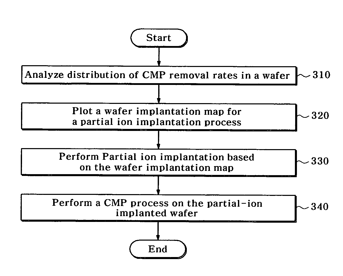
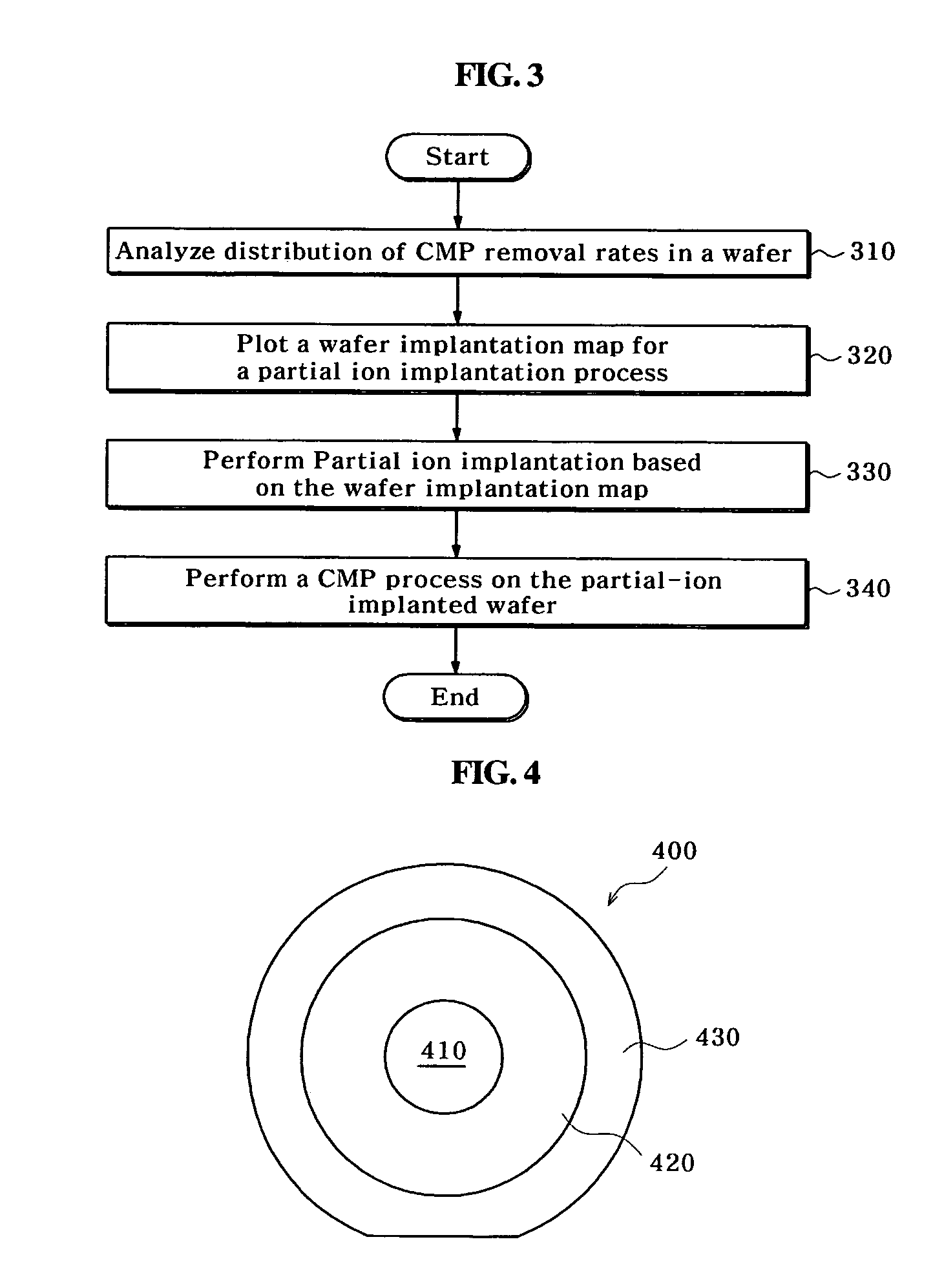
[0036]FIG. 3 is a flow chart illustrating a chemical mechanical polishing method for manufacturing a semiconductor device in accordance with the present invention.

[0037]Referring now to FIG. 3, distribution of a removal rate of the target film with respect to a chemical mechanical polishing of the wafer is first analyzed (Step 310). This step may be carried out using a test wafer. Next, a wafer implantation map is plotted for the partial ion implantation as a subsequent process (Step 320). Herein, the partial ion implantation process refers to a process involving dividing the wafer into at least two regions and performing ion implantation such that the respective regions are d...


PUM

PropertyMeasurementUnit
concentrationsaaaaaaaaaa
concentrationaaaaaaaaaa
flatnessaaaaaaaaaa

Abstract

Disclosed herein is a chemical mechanical polishing (CMP) method for manufacturing a semiconductor device, comprising performing partial ion implantation of dopants at different concentrations into a plurality of at least two divided regions of a wafer having a planarization-target film, and subjecting the partially ion implanted-wafer to a chemical mechanical polishing process. In accordance with the present invention, non-uniformity of the removal rate in a chemical mechanical polishing process is countervailed by dopants which are implanted at different concentrations via partial ion implantation, and thereby it is possible to polish the target film at a uniform removal rate.

Description

BACKGROUND OF THE INVENTION[0001]1. Field of the Invention[0002]The present invention relates to a method for manufacturing a semiconductor device, and more particularly to a chemical mechanical polishing method for manufacturing a semiconductor device.[0003]2. Description of the Related Art[0004]Recently, with the increased degree of integration of semiconductor devices and introduction of various materials, the importance of planarization processes has increased. Among such processes, mechanical polishing results in the formation of deformed layers, causing product defects, while chemical polishing does not cause the formation of such deformed layers, it has a limitation in that precise flatness cannot be achieved. As such, chemical mechanical polishing (CMP) is primarily employed which has the advantages of both chemical and mechanical polishing methods.[0005]In such a chemical mechanical polishing method, a wafer having a polishing-target film is polished by a pad and slurry. A ...

Claims


Application Information

Patent Timeline
Patent Type & Authority Patents(United States)
IPC IPC(8): H01L21/461H01L21/302
CPCH01L21/3212E03C1/122E03C2201/60
Inventor CHOI, YONG SOOLEE, WON MO
Owner SK HYNIX INC
Why Eureka
Try Eureka