Light-emitting element with porous light-emitting layers

a light-emitting layer and light-emitting element technology, applied in the field of light-emitting elements, can solve the problems of inability to further reduce the driving voltage, the performance of the quantum well to be limited, and the poor efficiency of the element, so as to reduce the concentration of doping, reduce the anti-static electricity ability, and improve the reliability of the elemen

Active Publication Date: 2007-09-18
GENESIS PHOTONICS
View PDF4 Cites 20 Cited by
  • Summary
  • Abstract
  • Description
  • Claims
  • Application Information

AI Technical Summary

Benefits of technology

[0010]By utilizing the light-emitting element of the invention, the driving voltage of the element can be decreased significantly, and so this light-emitting structure can be used to reduce the doping concentration in the light-emitting layer without affecting the driving voltage, thereby a preferred crystalline structure can obtained so that the anti-static electricity ability and element reliability can be improved.
[0011]Moreover, a plurality of porous light-emitting layers with different wavelengths may be grown on the light-emitting element of the invention, so as to elevate the performance of the light-emitting element effectively, and also to achieve a light-mixing element of a single chip, with the properties of high light-emitting benefit, high reliability, high light-mixing modularity and low cost and the like. Also, the porous light-emitting layer structure of the invention can overcome the shortage that a light-emitting element in the prior art can only emit a single wavelength. The light-emitting element of the invention can achieve the combination of the light-emitting layers with different light-emitting frequency spectrums to produce an efficient element with a high flexible light-mixing ratio.

Problems solved by technology

Reviewing the development history of the light-emitting diode, the earliest light-emitting layer structure is a simple P and N junction, but the efficiency is poor since the chance for an electron and a hole to recombine is not so high.
However, the disadvantage is that although most of the carriers can be captured and hence trapped in this quantum well without escaping, this carrier still has the ability to move in two-dimensional space, therefore resulting in the performance of the quantum well to be limited, including the disadvantages that the driving voltage cannot be further decreased, the anti-static electricity ability cannot be elevated effectively, and the light-emitting efficiency may be limited by the limited carrier recombination efficiency of the quantum well.
Moreover, although the light-emitting diode has become a widely available commercial product to date, the light-emitting diode found in the market is still limited to the property of single chip and single wavelength.

Method used


Image

  • Light-emitting element with porous light-emitting layers
  • Light-emitting element with porous light-emitting layers
  • Light-emitting element with porous light-emitting layers

Examples


first embodiment

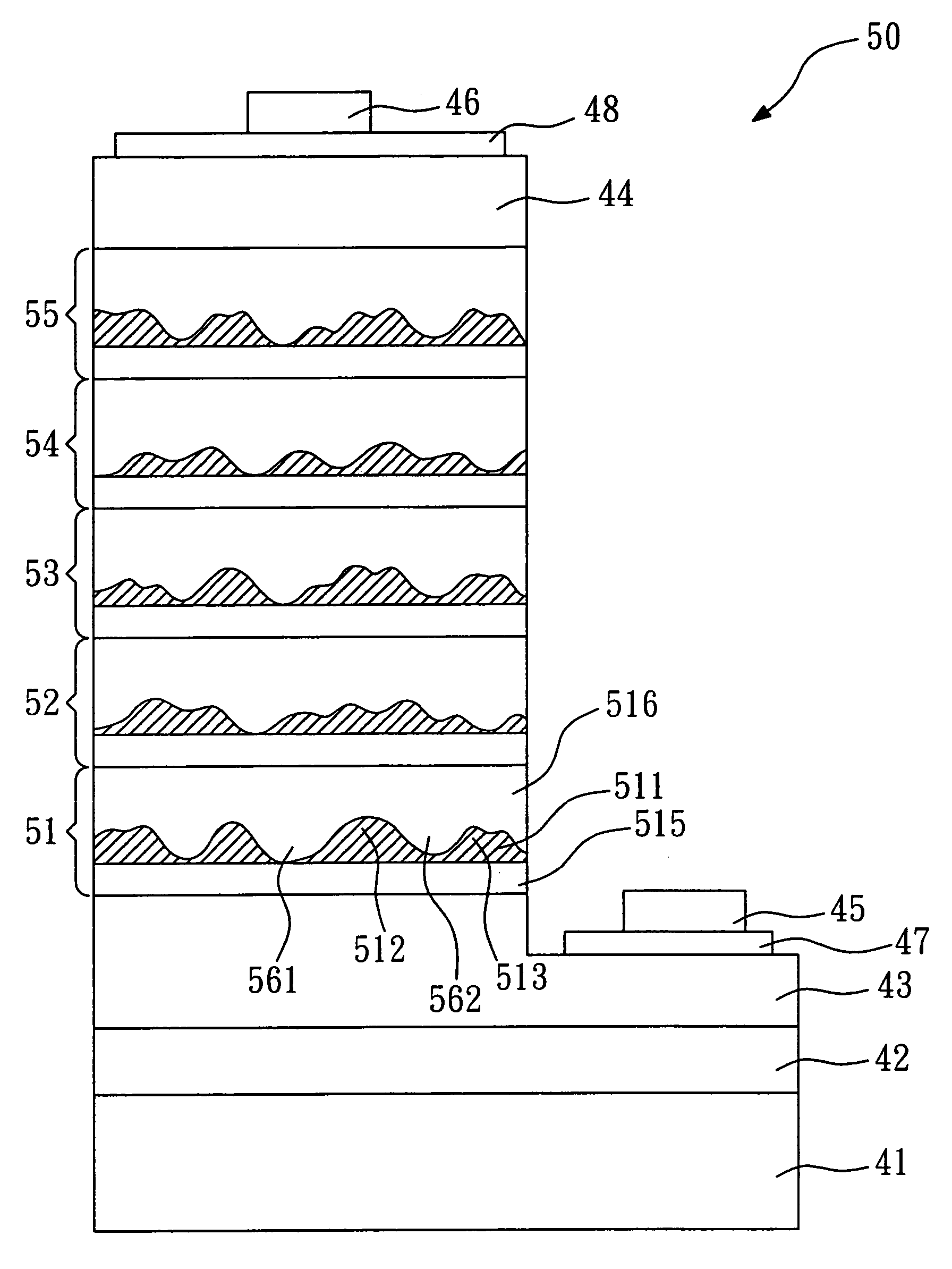
[0027]With reference to FIG. 4, it shows the construction of a light-emitting element 50 having porous light-emitting layers according to the present invention. The light-emitting element 50 includes a substrate 41, a buffer layer 42, a first conductive cladding layer 43, five porous light-emitting layers 51, 52, 53, 54 and 55, and a second conductive cladding layer 44.

[0028]The light-emitting 50 further includes two electrodes 45, 46 to be connected with the external power supply, wherein the preferred implemented material is aurum (Au). The buffer layer 42 is formed on the substrate 41. The first conductive cladding layer 43 formed on the buffer layer 42 may be an N-type cladding layer to provide electron. The second conductive cladding layer 44 that is formed on the porous light-emitting layers 55 may be a P-type cladding layer to provide holes. The first conductive cladding layer 43 and the second conductive cladding layer 44 are both of aluminum indium gallium nitride structure...

second embodiment

[0035]As shown in FIG. 5, the light-emitting element 60 according to the present invention is positioned between the N-type conductive cladding layer 43 and P-type conductive cladding layer 44, and includes five quantum well light-emitting layers doped with the silicon (Si) impurity 61, 62, etc., two porous light-emitting layers with a first wavelength 63, 64, etc., and two porous light-emitting layers with a second wavelength 65, 66.

[0036]The five quantum well light-emitting layers doped with the silicon (Si) impurity 61, 62, etc. are sequentially formed above the N-type conductive cladding layer 43. Taking the quantum well light-emitting layer 61 as an example, said quantum well light-emitting layer 61 has a quantum well structure 611 and two barrier layers 612 and 613.

[0037]Above the quantum well light-emitting layer doped with the silicon (Si) impurity 62 are sequentially the two porous light-emitting layers with the fist wavelength 63, 64. Taking the porous light-emitting layer...

third embodiment

[0045]As shown in FIG. 7, a light-emitting element 70 according to the present invention is positioned between the N-type conductive cladding layer 43 and P-type conductive cladding layer 44, and includes two quantum well light-emitting layers doped with the silicon (Si) impurity 71, 72, five porous light-emitting layers with a first wavelength 73, 74, etc., and two porous light-emitting layers with a second wavelength 75, 76.

[0046]Two quantum well light-emitting layers doped with the silicon (Si) impurity 71, 72, etc. are sequentially formed above the N-type conductive cladding layer 43. Taking the quantum well light-emitting layer 71 as an example, said quantum well light-emitting layer 71 has a quantum well structure 711 and two barrier layers 712, and 713.

[0047]The five porous light-emitting layers with the first wavelength 73, 74 are sequentially above the quantum well light-emitting layer doped with the silicon (Si) impurity 72. Taking the porous light-emitting layer with the ...


PUM

PropertyMeasurementUnit
radial lengthaaaaaaaaaa

Abstract

The invention relates to a light-emitting element with porous light-emitting layers. The light-emitting element comprises: a substrate, a first conductive cladding layer, a second conductive cladding layer and at least one porous light-emitting layer. The porous light-emitting layer is formed between the first conductive cladding layer and the second conductive cladding layer, and has an upper barrier layer, a lower barrier layer and a carrier trap layer. The carrier trap layer positioned between the upper barrier layer and the lower barrier layer has a plurality of chevron structures for defining a plurality of valley shaped structures, and is an indium-containing nitride structure, the energy band gap of which is less than those of the upper barrier layer and the lower barrier layer. By utilizing the light-emitting element of the invention, the driving voltage of the element can be decreased significantly; thereby a preferred crystalline structure can be obtained so that the anti-static electricity ability and element reliability could be improved. Moreover, a plurality of porous light-emitting layers with different wavelengths may be grown on the light-emitting element of the invention, so as to elevate the performance of the light-emitting element effectively, and also to achieve a light-mixing element of a single chip, meanwhile so as to obtain the properties of high light-emitting benefit, high reliability, high light-mixing modularity and low cost and the like.

Description

BACKGROUND OF THE INVENTION[0001]1. Field of the Invention[0002]The invention relates to a light-emitting element, specifically, a light-emitting element with porous light-emitting layers.[0003]2. Description of the Related Art[0004]In recent years, as the price of a light-emitting diode becomes cheaper and cheaper, various application products utilizing the properties of the light-emitting diode such as thin, light, short and small, power-saving, and multi-colorizing, become more and more popular, such as in various assistant back lights for electronic instrument decoration, automobile instrument panels, public decorative lamps, various indoor indicator lights, fascia advertisement lamp and the like. Looking into the future, it is not a dream that all of the existing light-emitting elements will be substituted by solid light-emitting diodes.[0005]Reviewing the development history of the light-emitting diode, the earliest light-emitting layer structure is a simple P and N junction, ...

Claims


Application Information

Patent Timeline
Patent Type & Authority Patents(United States)
IPC IPC(8): H01L27/01H01L27/15H01L33/12H01L33/32
CPCH01L33/18H01L33/08H01L33/32
Inventor CHEN, CHENG CHUAN
Owner GENESIS PHOTONICS
Why Eureka
Try Eureka