Wiring substrate for mounting semiconductor components

a semiconductor and substrate technology, applied in the field of wiring boards, can solve the problems of insufficient capacitance, insufficient wiring distance, and difficulty in maintaining power supply potential and ground potential stably, and achieve the effects of low resistance, insufficient machining accuracy, and low inductan

Inactive Publication Date: 2007-09-18
KYOCERA CORP
View PDF8 Cites 21 Cited by
  • Summary
  • Abstract
  • Description
  • Claims
  • Application Information

AI Technical Summary

Benefits of technology

[0019]The wiring board and semiconductor device with this structure have the capacitor accommodated in the cavity and allow the electrode terminals on the upper surface of the capacitor to be directly connected to the semiconductor component mounted on the wiring board, which enables the decoupling capacitor to be connected to a semiconductor component with low resistance and low inductance. Accordingly, rapid charge transfer between the capacitor and semiconductor component is enabled, and malfunctions of the semiconductor component due to instability of power supply voltage can be prevented. In addition, power supply noise can be effectively suppressed.
[0021]When the connection portion comprises electrode terminals provided on the back surface of the capacitor, the connection between the capacitor and the wiring board can also be made with low resistance and low inductance, allowing rapid charge transfer from the power supply to the capacitor. As a result, malfunctions of the semiconductor component due to instability of the power supply voltage can be prevented.
[0023]In cases where the adhesive layer is employed, it is preferable that the adhesive layer comprises a material that melts by heating. This is because when the semiconductor component is mounted on the wiring board, the adhesive layer is melted by heat, enabling self-alignment between the capacitor and the semiconductor component. Accordingly, even if the machining accuracy on the capacitor is low, required positioning accuracy with respect to the semiconductor component can be secured and occurrence of contact failure of the capacitor can be prevented. In addition, since there is no need for jigs for positioning from outside, the mounting cost can be reduced. Furthermore, even if the thermal expansion coefficient of the capacitor embedded in the cavity and that of the build-up layer around the capacitor differ, peeling, cracking or break does not occur, and break or the like caused by insufficient machining accuracy on the wiring board and capacitor does not occur.
[0029]The wiring board and the semiconductor component of the structure above are arranged such that the capacitor is accommodated in the cavity of the build-up layer through the surface wiring layer which is provided on the upper surfaces of the build-up layer and the capacitor, and the semiconductor component is mounted on a position immediately above the capacitor in the surface wiring layer. Accordingly, the electrode terminals of the capacitor can be connected to the semiconductor component mounted on the surface wiring layer through the wiring conductor layers in the surface wiring layer in a short distance. This enables the capacitor and the semiconductor component to be connected with low resistance and low inductance. In addition, the connection between the capacitor and the wiring board can be made through the wiring layers in the surface wiring layer in a short distance. As a result, charge transfer from the power supply through the capacitor to the semiconductor component can be accomplished rapidly, so that malfunctions of the semiconductor component due to instability of the power supply can be prevented. Moreover, even if the thermal expansion coefficient of the capacitor embedded in the cavity and that of the build-up layer around the capacitor differ, peeling, cracking or break does not occur, and break or the like caused by insufficient machining accuracy on the wiring board and capacitor does not occur.

Problems solved by technology

As the wiring distance for electrically connecting the decoupling capacitor and semiconductor component lengthens, due to the resistance and inductance that the wiring has, it becomes difficult to maintain power supply potential and ground potential stably.
However, although the approach for forming a decoupling capacitor by utilizing conductive layers and dielectric layers allows the wiring distance to be shortened, because of small dielectric constant of the dielectric layers, it has the drawback that the capacitance is insufficient compared to when a chip capacitor is used.
However, when the structure in which the chip capacitor is buried inside the wiring board is employed, peeling, cracking or break due to difference in thermal expansion coefficient between the buried chip capacitor and the material of the wiring board around the chip capacitor, and break due to clearance caused by insufficient machining accuracy on the wiring board and chip capacitor would occur.
Also, when the structure in which the chip capacitor is embedded in the cavity formed on the surface of the wiring board, because the bottom surface of the cavity for embedding the chip capacitor reaches inside the wiring board, the structure does not allow the capacitor to directly connect to a conductive wiring layer on the surface of the wiring board, and the connection is made via a conductive wiring layer on the back side of the wiring board.
As a result, the wiring distance lengthens.
Thus, realistically, inserting a chip capacitor is difficult, and this method can be applied to only limited applications that permit a large bump pitch.

Method used


Image

  • Wiring substrate for mounting semiconductor components
  • Wiring substrate for mounting semiconductor components
  • Wiring substrate for mounting semiconductor components

Examples


example 1

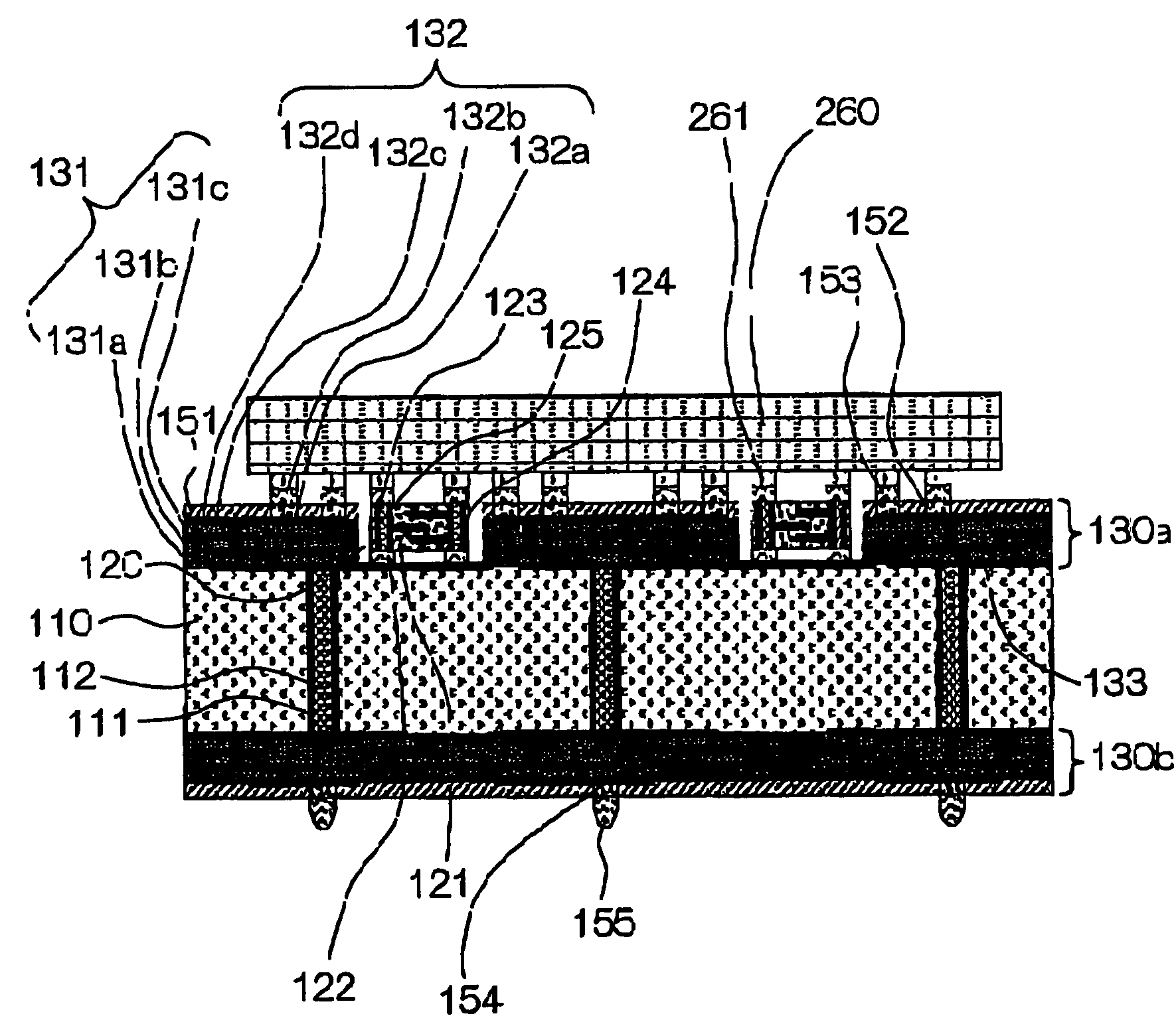
[0093]The wiring board shown in FIGS. 1 and 2 was produced. The production process was as follows.[0094](1) A glass epoxy resin-impregnated base material was used for the core substrate 110. Prior to the formation of the build-up layer 130a, the core substrate 110 was provided with holes for the through-holes by drilling or laser machining. It is also possible to carry out desmear by a plasma treatment when the need arises.[0095](2) Subsequently, a copper-plated film was formed on the surface of the core substrate 110 by electroless copper plating. Then, the whole of the core substrate 110 was dipped in the electroless copper plating liquid to further form a copper-plated film using the foregoing copper-plated film as the electrode.

[0096]Subsequently, a photosensitive dry film is attached to the surface of the aforementioned copper-plated film, which was then subjected to masked exposure followed by development with an alkali solution so that a resist-plated film with a predetermine...

example 2

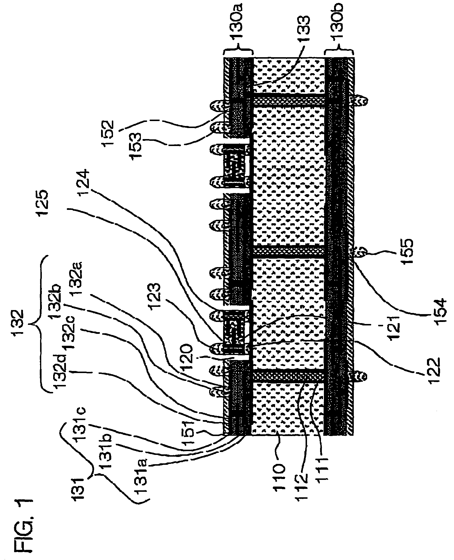
[0115]Subsequently, the wiring board shown in FIGS. 3 and 4 was produced. The production process thereof will be described referring to FIGS. 3 and 4. The production steps that are the same as the steps in the example of FIGS. 1 and 2 are omitted as far as possible, and the steps characteristic of the present example 2 are described in detail.

[0116]First, the core substrate 110 having holes for through-holes was fabricated as in the example 1. Then, the wiring conductor layer 132a comprising a copper film and the through-hole interior surface wiring layers 111 were formed in the surface of the core substrate 110. Then, the surface of the copper film and the surfaces of the through-hole 111 lands were roughened, and a resin filler was injected into the through-holes 112.

[0117]The wiring conductor layer 132a functions also as stopper layer for the laser machining for cavity formation described later. Any of the wiring conductor layers 132 that are hereinafter successively stacked may ...

example 3

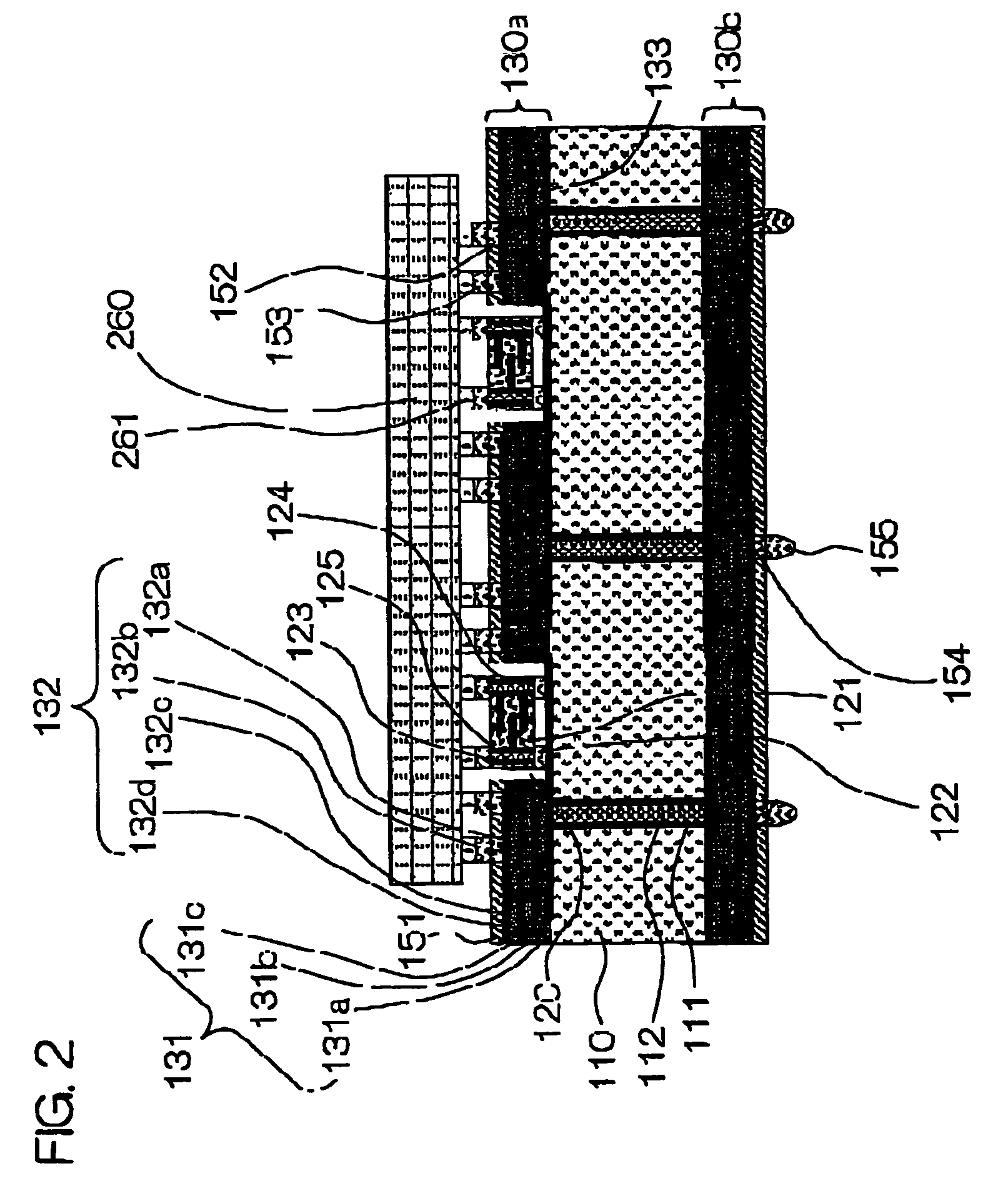
[0132]Subsequently, the wiring board shown in FIGS. 5, 6 and 7 was produced. The production process thereof will be described. The production steps that are the same as the steps in the example of FIGS. 1 to 4 are omitted as far as possible, and the steps characteristic of the present example 3 are described in detail.

[0133]Referring to FIG. 5, the core substrate 110 having holes for through-holes was fabricated. Then, the wiring conductor layer 132a comprising a copper film formed on the surface of the core substrate 110 and the through-hole interior surface wiring layers 111 were formed. Then, the surface of the copper film and the surfaces of the through-hole lands were roughened, and a resin filler was injected into the through-holes 112.

[0134]The wiring conductor layer 132a functions also as stopper layer during the laser machining for cavity formation as described later. Any of the wiring conductor layers 132 that are hereinafter successively stacked may be used as the stopper...


PUM


Abstract

There is disclosed a wiring board comprising a core substrate 110, a build-up layer 130a formed on at least one side of main surfaces the core substrate, wherein a cavity 120 for accommodating a chip-type decoupling capacitor 121 is formed in the build-up layer 130a. The capacitor 121 includes electrode terminals on an upper surface thereof that are directly connected to a semiconductor component, and electrode terminals on a back surface of the capacitor 121 is connected to a wiring conductor layer 132a on a bottom surface of the cavity 120. This structure enables decoupling capacitor and the semiconductor component 260 to be connected with low resistance and low inductance.

Description

[0001]This application is based on applications Nos. JP2003-304518, JP2003-304519 and JP2003-337504 the content of which is incorporated hereinto by reference.BACKGROUND OF THE INVENTION[0002]1. Field of the Invention[0003]The present invention relates to wiring boards for mounting semiconductor components such as semiconductor integrated circuit chips (LSI chips) used for information processing devices such as computers.[0004]In particular, the present invention relates to a wiring board with a decoupling capacitor used as a power supply provided in the vicinity of a semiconductor component, which allows the semiconductor component to operate stably and speedily, and a semiconductor device comprising the wiring board and semiconductor component mounted thereon.[0005]2. Description of the Related Art[0006]Conventionally, in order to operate a semiconductor component speedily and stably, studies have been devoted to stabilizing supply potential and ground potential to the semiconduct...

Claims


Application Information

Patent Timeline
Patent Type & Authority Patents(United States)
IPC IPC(8): H01L23/06H01L23/02H01L23/48H01L23/50H05K1/18H05K3/46
CPCH01L23/50H05K1/183H05K1/185H01L2224/16225H01L2924/01078H01L2924/01079H01L2924/15311H05K3/4602H05K3/4697H01L2924/01019H01L2224/05568H01L2224/05573H01L2224/16265H01L2924/00014H01L2924/15159H01L2924/19103H01L2924/19104H01L2224/05599
Inventor NISHIKAWA, HIROYUKITANAHASHI, SHIGEOHAYASHI, KATSURA
Owner KYOCERA CORP
Why Eureka
Try Eureka