Power semiconductor device package

a technology of semiconductor devices and semiconductor devices, applied in semiconductor devices, semiconductor/solid-state device details, electrical equipment, etc., can solve the problems of increasing output capacity, difficult to reduce the size of a power supply circuit, and large loss of conductan

Inactive Publication Date: 2007-09-18
KK TOSHIBA
View PDF8 Cites 72 Cited by
  • Summary
  • Abstract
  • Description
  • Claims
  • Application Information

AI Technical Summary

Problems solved by technology

The conduction loss generally becomes large along with the increase in the output capacity and the rated current of the power supply circuit.
As a result, it has been difficult to reduce the size of a power supply circuit because the package size of a power MOSFET is increased as the capacity of the power supply circuit becomes large.

Method used


Image

  • Power semiconductor device package
  • Power semiconductor device package
  • Power semiconductor device package

Examples


first embodiment

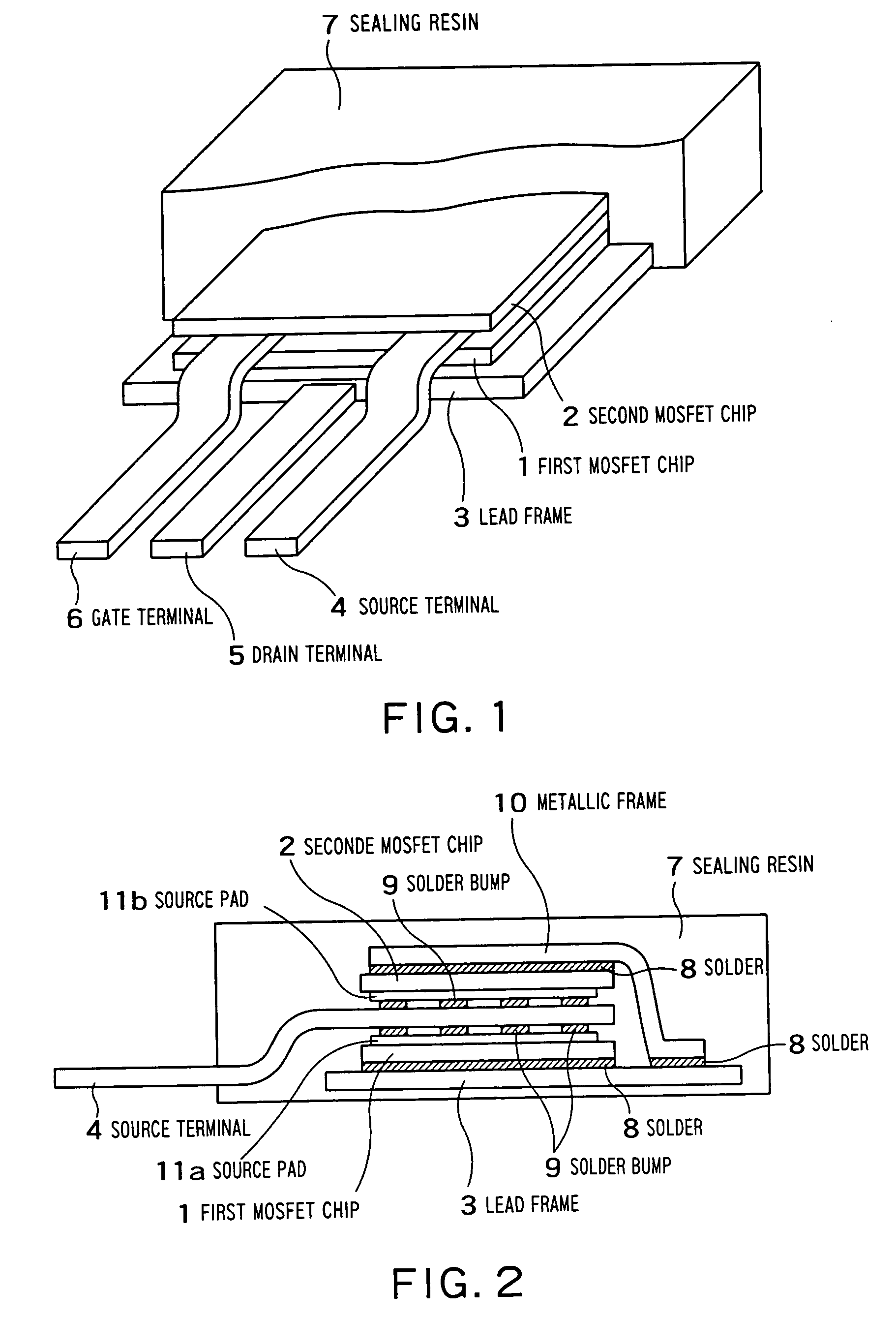
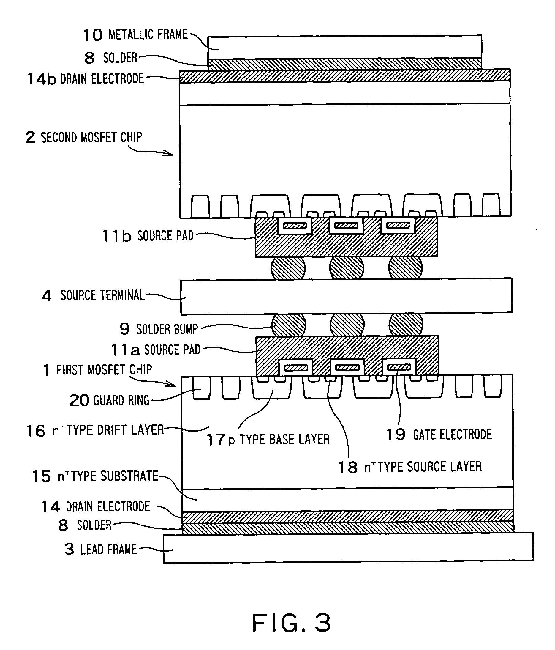
[0031]The power semiconductor device package according to the present invention comprises: a lead frame 3; a first power MOSFET chip 1 which is mounted on the lead frame 3 with solder 8 as a thermoplastic conductive member; a drain terminal 5 which is extended from the lead frame 3, and connected to a drain electrode on the back of the first power MOSFET chip 1; a source pad 11a and a gate pad (not shown) formed on the first power MOSFET chip 1; a source terminal 4 and a gate terminal 6 in each of which one side is connected to the source pad 11a and the gate pad on the first power MOSFET chip 1 with solder bumps 9 as a thermoplastic conductive member, respectively; a second power MOSFET chip 2 which is connected to the first power MOSFET chip 1 in parallel by connecting a source pad 11b and a gate pad (not shown) formed on the surface to the other side of the source terminal 4 and the gate terminal 6 with solder bumps 9, respectively, and a drain electrode on the back to the lead f...

second embodiment

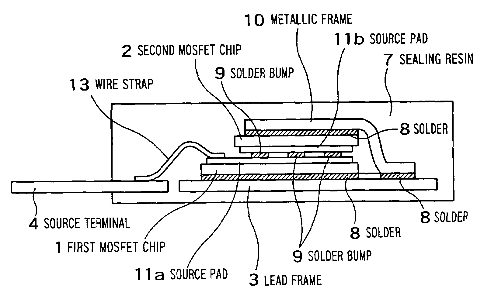
[0051]The power semiconductor device package according to the present invention comprises: a lead frame 3; a first power MOSFET chip 1 which is mounted on the lead frame 3 with solder 8; a drain terminal 5 which is extended from the lead frame 3, and connected to a drain electrode on the back of the first power MOSFET chip 1; a source pad 11a and a gate pad (not shown) formed on the first power MOSFET chip 1; a second power MOSFET chip 2 which is connected to the first power MOSFET chip 1 in parallel by connecting a source pad 11b and a gate pad (not shown) formed on the surface to the source pad 11a and the gate pad on the first power MOSFET chip 1 with solder bumps 9, respectively, and a drain electrode on the back to the lead frame 3 with a metallic frame 10 and the solder 8, and is arranged opposing to the first power MOSFET chip 1; wire straps 13 which connect the source pad 11a on the first power MOSFET chip 1 and a source terminal 4 as an external terminal, and the gate pad o...

third embodiment

[0063]FIG. 7 is a partial cutaway perspective view showing the structure of a power semiconductor device package according to the present invention.

[0064]While the wire straps 13 are used for connection between the source pad 11a (refer to FIG. 5) on the first power MOSFET chip 1 and the source terminal 4, and connection between the gate pad on the first power MOSFET chip 1 and the gate terminal 4 in the power semiconductor device package of the second embodiment of the present invention shown in FIGS. 4 and 5, bonding wires 21 are used for the connection in the power semiconductor device package according to the third embodiment of the present invention shown in FIG. 7.

[0065]Since the electrode wiring metallic plates 4 and 6 are not sandwiched between the first and second power MOSFET chips 1 and 2, the manufacturing process technically becomes easy, and is simplified even in the power semiconductor device package according to the third embodiment of the invention.

[0066]Here, in or...


PUM


Abstract

A power semiconductor device package according to one aspect of the present invention comprises: a plurality of power semiconductor chips which are arranged in a laminated structure so that the plurality of power semiconductor chips are opposing to each other at the surfaces with the same electrical structures, and which are connected in parallel to one another, and are sealed in a sealing resin as one body.

Description

CROSS REFERENCE TO RELATED APPLICATION[0001]The subject application is related to subject matter disclosed in Japanese Patent Application No. 2004-115728 filed on Apr. 9, 2004 in Japan to which the subject application claims priority under Paris Convention and which is incorporated herein by reference.BACKGROUND OF THE INVENTION[0002]1. Field of the Invention[0003]The present invention relates to a power semiconductor device package.[0004]2. Related Background Art[0005]The size and the power loss of a power supply circuit have been reduced along with the development and improvement of the power semiconductor device. The conduction loss of, especially, an AC adapter and the like has been decreased by reducing the on-resistance of a power metal oxide semiconductor field-effect transistor (power MOSFET) which is a switching element mainly used as one of components, and reduction in the power loss of the adapter and the like has been realized.[0006]Since the on-resistance of the power M...

Claims


Application Information

Patent Timeline
Patent Type & Authority Patents(United States)
IPC IPC(8): H01L23/02H01L25/07H01L23/495H01L25/18
CPCH01L23/49575H01L24/40H01L24/41H01L2924/1306H01L2224/40247H01L2224/73253H01L2224/73221H01L2224/32245H01L2924/01033H01L2924/01006H01L24/48H01L24/45H01L2924/13091H01L2924/01082H01L2924/01029H01L2924/01015H01L2924/01013H01L2225/06562H01L2224/48472H01L2224/48247H01L2224/48091H01L2224/45147H01L25/074H01L2224/45014H01L2224/45124H01L2924/00014H01L2924/00H01L2924/181H01L2224/40245H01L2224/73257H01L2224/84801H01L2224/37124H01L2224/37147H01L2224/83801H01L24/37H01L24/84H01L2924/00012
Inventor SAITO, WATARUOMURA, ICHIRO
Owner KK TOSHIBA
Why Eureka
Try Eureka