Carrier for wafer-scale package and wafer-scale package including the carrier

a carrier and wafer-scale technology, applied in the field of carrier substrates, can solve the problems of high likelihood of failure of semiconductor devices, method and device of '885 patent, and bond types that may fail during operation

Inactive Publication Date: 2007-09-18
MICRON TECH INC
View PDF33 Cites 67 Cited by
  • Summary
  • Abstract
  • Description
  • Claims
  • Application Information

AI Technical Summary

Benefits of technology

[0012]The carrier substrate may also include conductive traces extending substantially laterally from selected ones of the electrically conductive vias. Preferably, each laterally extending conductive trace is carried by the carrier substrate proximate a surface opposite the surface to which a semiconductor device may be secured, which opposite surface is also referred to herein as a back side surface or simply as a back side of the carrier substrate. Such laterally extending conductive traces facilitate reconfiguration of the electrical paths through the carrier substrate.
[0021]Conductive material may be disposed in each of the apertures to define vias through the carrier substrate or substrate wafer. As conductive material is disposed within each of the apertures, the conductive material and the material of the bond pad exposed to the aperture may diffuse and thereby at least partially secure the semiconductor device wafer and the substrate wafer to one another.

Problems solved by technology

Due to the typical use of a carrier substrate that has a different coefficient of thermal expansion than the semiconductor substrate of the semiconductor device, these types of bonds may fail during operation of the semiconductor device.
The method and devices of the '885 patent are, however, somewhat undesirable.
Thus, the likelihood of failure of the semiconductor device is undesirably high.
These circuits may undesirably alter the electrical characteristics of signals transmitted through the bond pads.
The testing of individual packaged semiconductor devices is, however, somewhat undesirable since each package must be individually aligned with such testing or probing equipment.

Method used


Image

  • Carrier for wafer-scale package and wafer-scale package including the carrier
  • Carrier for wafer-scale package and wafer-scale package including the carrier
  • Carrier for wafer-scale package and wafer-scale package including the carrier

Examples


Embodiment Construction

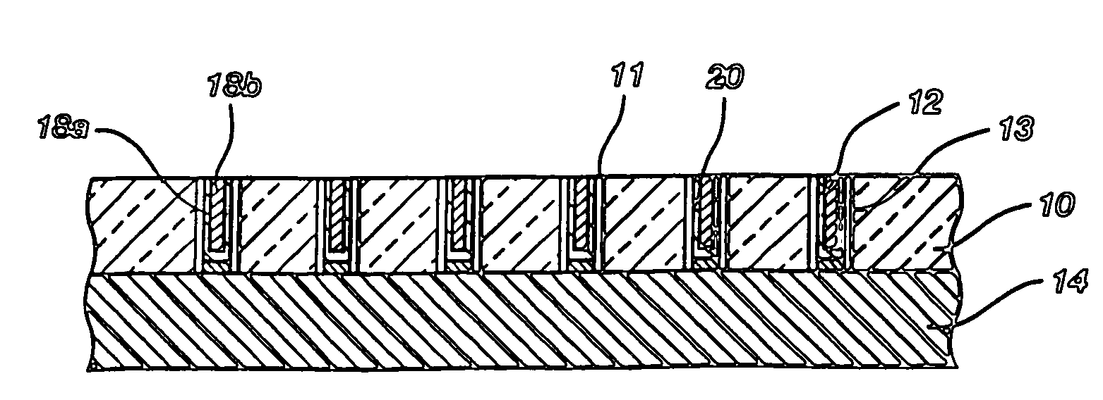
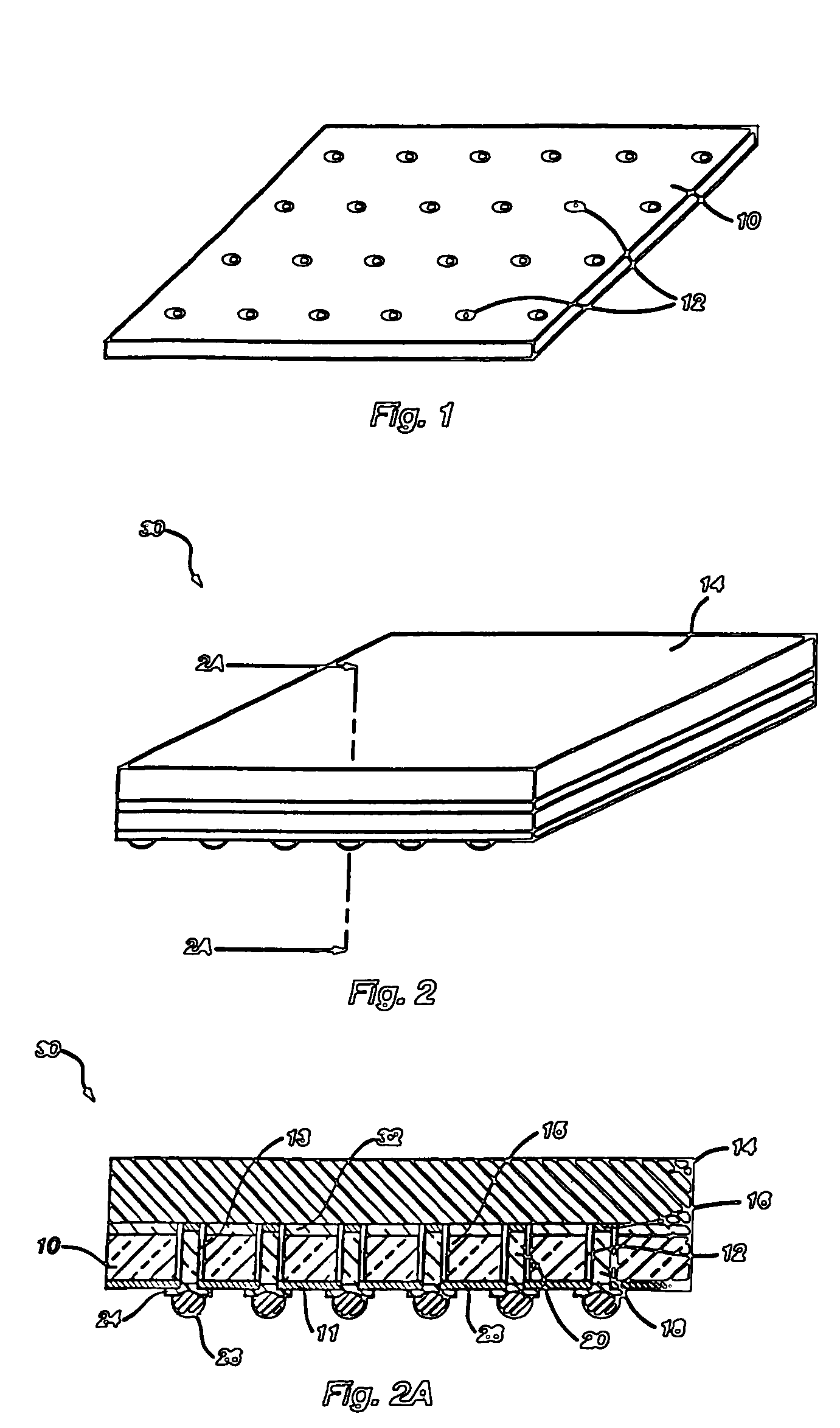
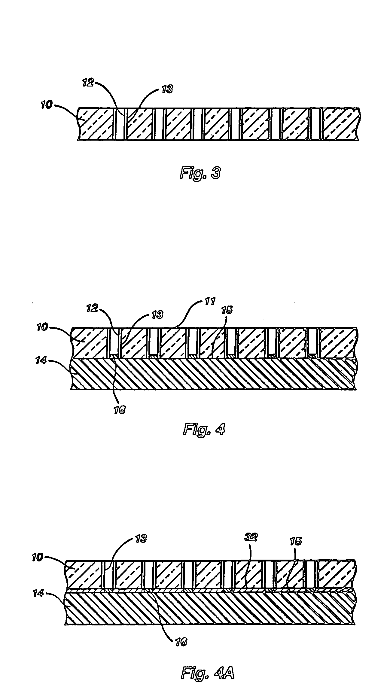
[0042]With reference to FIG. 1, a carrier substrate 10, which is also referred to herein as a semiconductor substrate or simply as a carrier, is illustrated. Carrier substrate 10 is a substantially planar structure that may be fabricated from a semiconductor material, such as silicon. An array of apertures 12 is defined through carrier substrate 10. Preferably, apertures 12 correspond substantially to the bond pads 16 (see FIG. 2A) of a semiconductor device 14 to be assembled with carrier substrate 10.

[0043]Turning to FIG. 2A, which illustrates a chip-scale package 30 including carrier substrate 10 and an associated semiconductor device 14, carrier substrate 10 may also include a quantity of conductive material 18 in each of apertures 12. Each aperture 12, which is coated with an insulative layer 13, and the conductive material 18 therein collectively define an electrically conductive via 20 that extends substantially through carrier substrate 10 and through which signals may be com...


PUM


Abstract

A carrier for use in a chip-scale package, including a semiconductor substrate, such as a semiconductor wafer, with a plurality of apertures formed therethrough. The present invention also includes a chip-scale package including the carrier. When the carrier is employed in such a package, a semiconductor device or a wafer including a plurality of semiconductor devices thereon is invertedly aligned with and disposed over the carrier so that bond pads of the semiconductor device or semiconductor devices substantially align with apertures through the semiconductor substrate. The chip-scale package also includes conductive material disposed in each of the apertures of the semiconductor substrate to form vias through the semiconductor substrate. Conductive traces may extend substantially laterally from selected vias. The chip-scale package may also include a contact or conductive bump disposed in communication with each via. An intermediate layer may be disposed between the semiconductor device and the semiconductor substrate. The intermediate layer may secure the semiconductor device to the semiconductor substrate and insulate structures of the semiconductor device. An insulative layer may be disposed on the semiconductor substrate opposite the semiconductor device. If the chip-scale package includes an intermediate layer or an insulative layer, the electrically conductive vias that extend through the semiconductor substrate are preferably exposed through such layers. The present invention also includes methods of fabricating the semiconductor substrate and assembling a chip-scale package of the invention, including substantially simultaneously assembling semiconductor devices and carrier substrates on a wafer-scale and singulating individual chip-scale packages from the assembled wafers.

Description

BACKGROUND OF THE INVENTION[0001]1. Field of the Invention[0002]The present invention relates to carrier substrates for use in chip-scale packages and to chip-scale packages including such carrier substrates. Particularly, the present invention relates to silicon carrier substrates. Methods of fabricating chip-scale packages are also within the scope of the present invention.[0003]2. Background of Related Art[0004]In conventional semiconductor device fabrication processes, a number of distinct semiconductor devices, such as memory chips or microprocessors, are fabricated on a semiconductor substrate, such as a silicon wafer. After the desired structures, circuitry, and other features of each of the semiconductor devices have been fabricated upon the semiconductor substrate, the substrate is typically singulated to separate the individual semiconductor devices from one another.[0005]Various post-fabrication processes, such as testing the circuits of each of the semiconductor devices ...

Claims


Application Information

Patent Timeline
Patent Type & Authority Patents(United States)
IPC IPC(8): H01L23/48H01L23/52H01L29/40H01L23/14H01L23/485H01L23/498
CPCH01L23/147H01L23/49827H01L24/13H01L24/10H01L2224/13099H01L2924/01013H01L2924/01022H01L2924/01079H01L2924/14H01L2924/01005H01L2924/01006H01L2924/01033H01L2924/014H01L2924/00H01L2924/12042H01L2224/13H01L2224/05026H01L2224/05001H01L2224/05572H01L2924/00014H01L24/11H01L24/03H01L2224/06131H01L24/05H01L2224/05644H01L2224/05099
Inventor AKRAM, SALMAN
Owner MICRON TECH INC
Why Eureka
Try Eureka