
Display device and a method of manufacturing the display device

a display device and display device technology, applied in the field of display devices, can solve problems such as difficulty in adopting the constitution

Active Publication Date: 2007-09-18
JOLED INC
View PDF10 Cites 54 Cited by
  • Summary
  • Abstract
  • Description
  • Claims
  • Application Information

AI Technical Summary

Benefits of technology

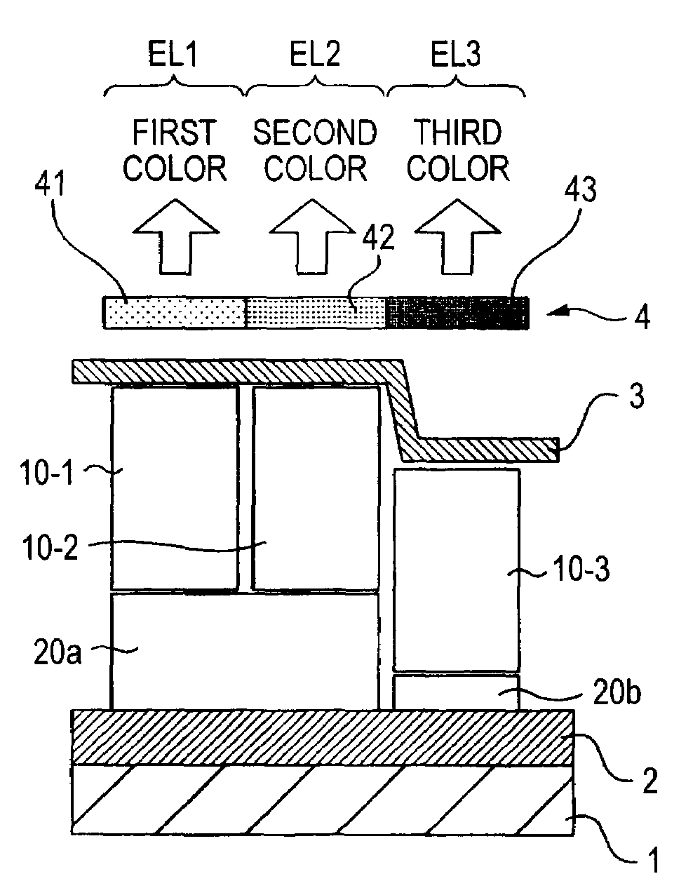
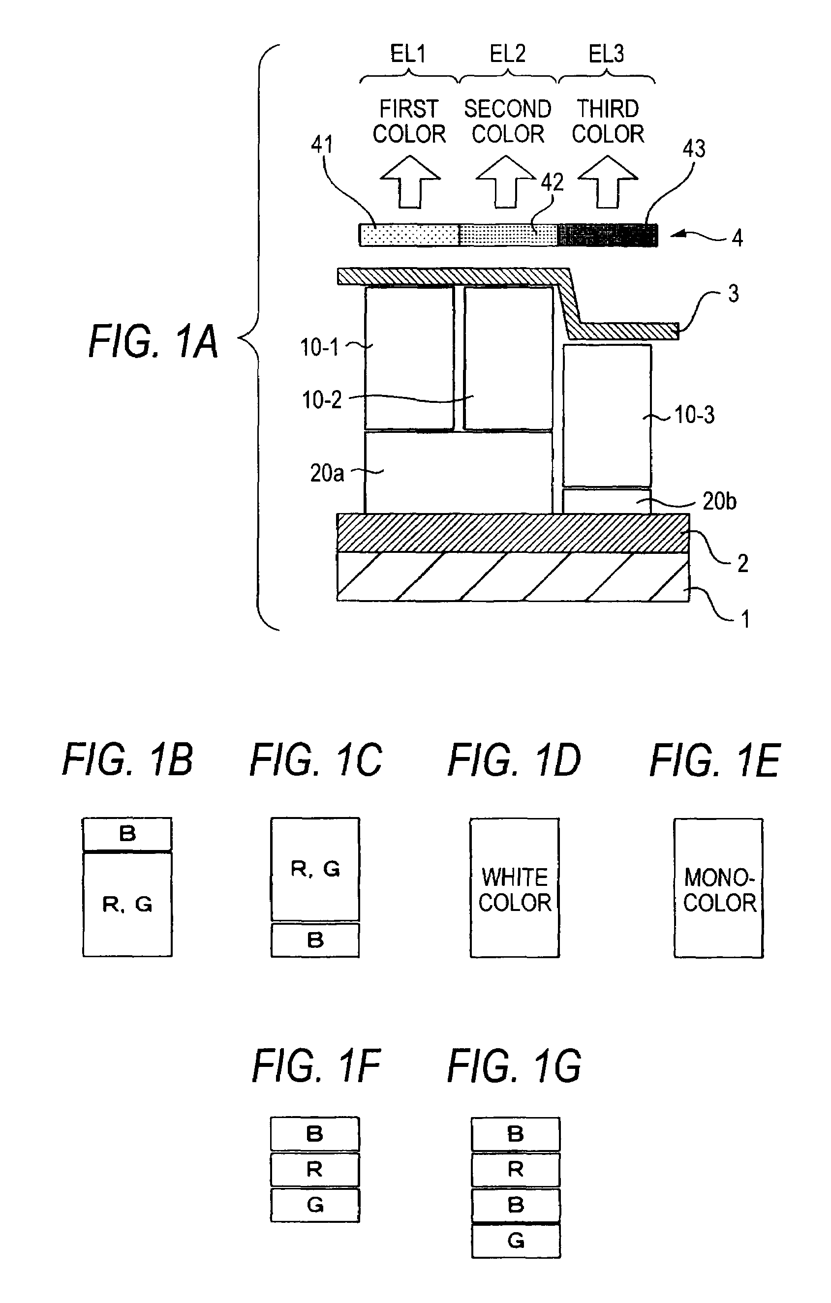
"The present invention is about a display device with a resonator structure that makes it difficult to set the optical distance. The invention proposes a solution by setting the optical distance of the cavity portion in a first light-emitting element of a pixel to be equal with the optical distance of the cavity portion in a second light-emitting element of the pixel, and making the optical distance of the cavity portion in the first light-emitting element different from the optical distance of the cavity portion in a third light-emitting element. This allows for easy and accurate setting of the optical distance and enables highly fine display with full color display excellent in color reproducibility."

Problems solved by technology

However, in the display device having a resonator structure of resonating a light emitted from a light-emitting layer, since the setting for the optical distance is complicated, it is difficult to adopt the constitution described above.

Method used


Image

  • Display device and a method of manufacturing the display device
  • Display device and a method of manufacturing the display device
  • Display device and a method of manufacturing the display device

Examples


example

[0071]Then, procedures for manufacturing display devices of concrete examples of the invention and comparative examples relative to the example are to be described, and the results of evaluation for them are to be described subsequently.

Manufacture of a Display Device of Examples

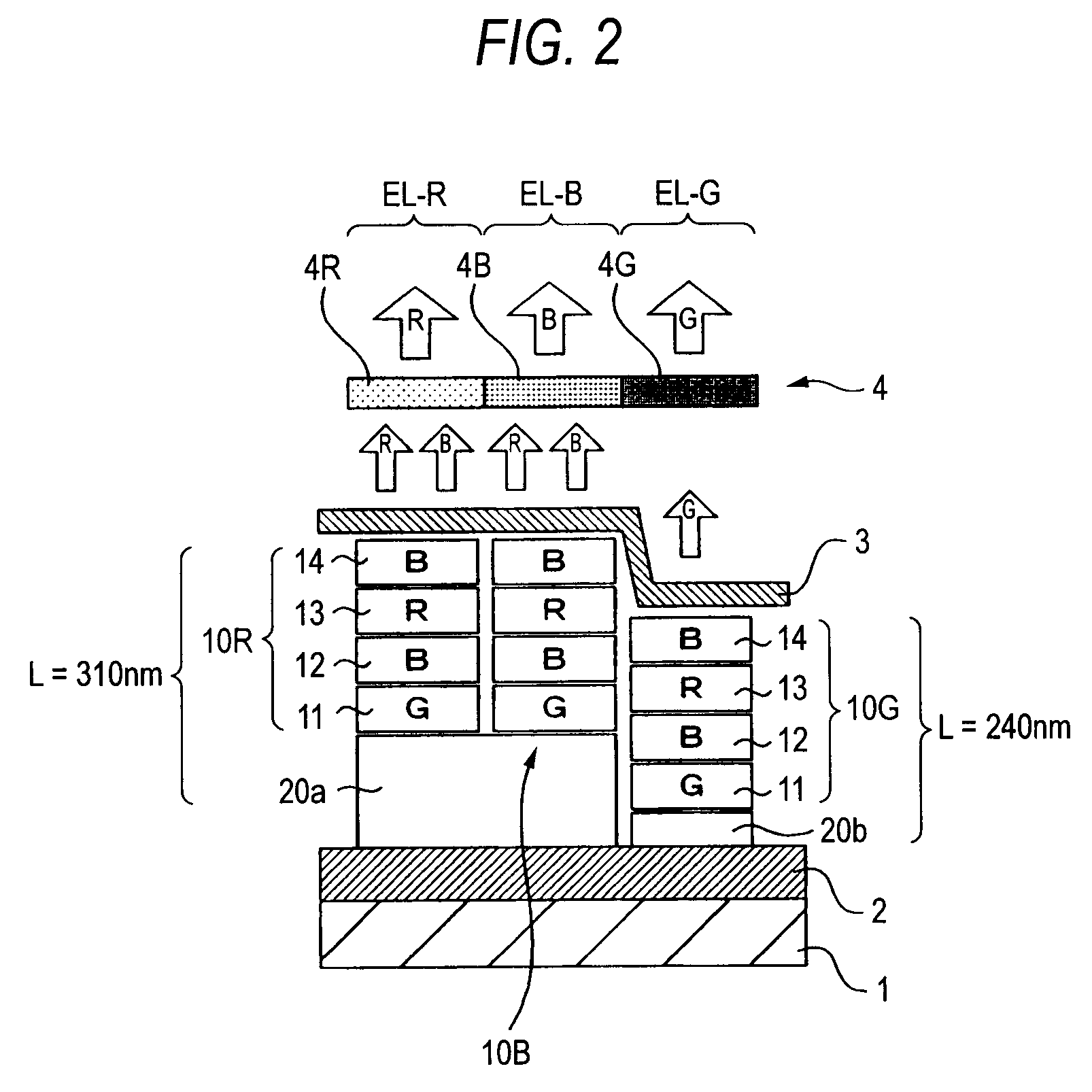
[0072]A lower electrode 2 comprising APC (Ag—Pd—Cu) (about 100 nm film thickness) for the anode as the mirror, and transparent conductive films 20a and 20b comprising ITO of each film thickness were formed on a substrate 1 comprising a glass plate as a pattern. Then, regions of the transparent conductive films 20a and 20b other than the light-emitting region of 2 mm×2 mm at the central portion on the surface were covered with an insulative film (not illustrated).

[0073]Then, a metal mask having an opening was located above and in the vicinity of the substrate 1 over an exposed portion of the transparent conductive films 20a and 20b forming each of the light-emitting regions. Light-emitting units 11 to 14 were...


PUM


Abstract

A display device having a light-emitting element which has a lower electrode, an upper electrode, a functional layer, and a cavity in which light generated in the functional layer is resonated wherein the optical distance of the cavity portion in a first light-emitting element is made equal with the optical distance of the cavity portion in a second light-emitting element, and the optical distance of the cavity portion in the first light-emitting element is different from the optical distance of the cavity portion in a third light-emitting element.

Description

CROSS REFERENCE TO RELATED APPLICATIONS[0001]The present invention contains subject matter related to Japanese Patent Application JP 2005-117717 filed in the Japanese Patent Office on Apr. 15, 2005, and Japanese Patent Application JP 2005-143472 filed in the Japanese Patent Office on May 17, 2005, the entire contents of which being incorporated herein by reference.BACKGROUND OF THE INVENTION[0002]1. Field of the Invention[0003]The present invention concerns a display device and a method of manufacturing the same and, more particularly, it relates to a self-light emitting display device in which light emitting elements such as organic EL elements are arranged on a substrate, and a method of manufacturing the same.[0004]2. Description of the Related Art[0005]A full color display device using light-emitting elements includes a constitution having a color filter in combination with a white light emitting element. One of the constitutions of the white light-emitting element is that a plu...

Claims


Application Information

Patent Timeline
Patent Type & Authority Patents(United States)
IPC IPC(8): H01L51/54
CPCH01L51/5265H01L27/3211H01L51/5036H10K59/35H10K50/125H10K59/876H05B33/22H05B33/10H10K50/852
Inventor MATSUDA, EISUKEASAKI, REO
Owner JOLED INC
Learn More