Method and apparatus for inspecting defects

a defect detection and defect technology, applied in the field of optical systems, can solve the problems of inability to detect defects in the mask surface with a high sensitivity, the vertical resolution perpendicular to the direction of shearing is not increased, and the difference between the two branched optical paths can be caused, so as to achieve enhanced inspection sensitivity and increase the horizontal resolution

Inactive Publication Date: 2007-09-18
HITACHI HIGH-TECH CORP
View PDF5 Cites 2 Cited by
  • Summary
  • Abstract
  • Description
  • Claims
  • Application Information

AI Technical Summary

Benefits of technology

[0012]Further, according to the present invention, the horizontal resolution is increased by controlling the amplitude and phase of a zero-order beam so that the inspection sensitivity is enhanced.

Problems solved by technology

As a result, a difference between the two branched optical paths can be caused by a disturbance or vibration applied from moving parts.
This fluctuation in interference intensity becomes a noise component when detecting defects in the mask surface, so that the defects in the mask surface cannot be detected with a high sensitivity.
However, the vertical resolution perpendicular to the direction of shearing is not increased.
Therefore, the vertical resolution comes to have a directional characteristic, causing such a problem in that the inspection sensitivity varies according to the direction of defects to be inspected.
However, an interference optical system is designed to manifest any irregularity (optical path difference), so that, in the case of a wafer using a metal wiring process, such a manifestation of this type of irregularity by the interference optical system becomes a disadvantage.

Method used


Image

  • Method and apparatus for inspecting defects
  • Method and apparatus for inspecting defects
  • Method and apparatus for inspecting defects

Examples


Embodiment Construction

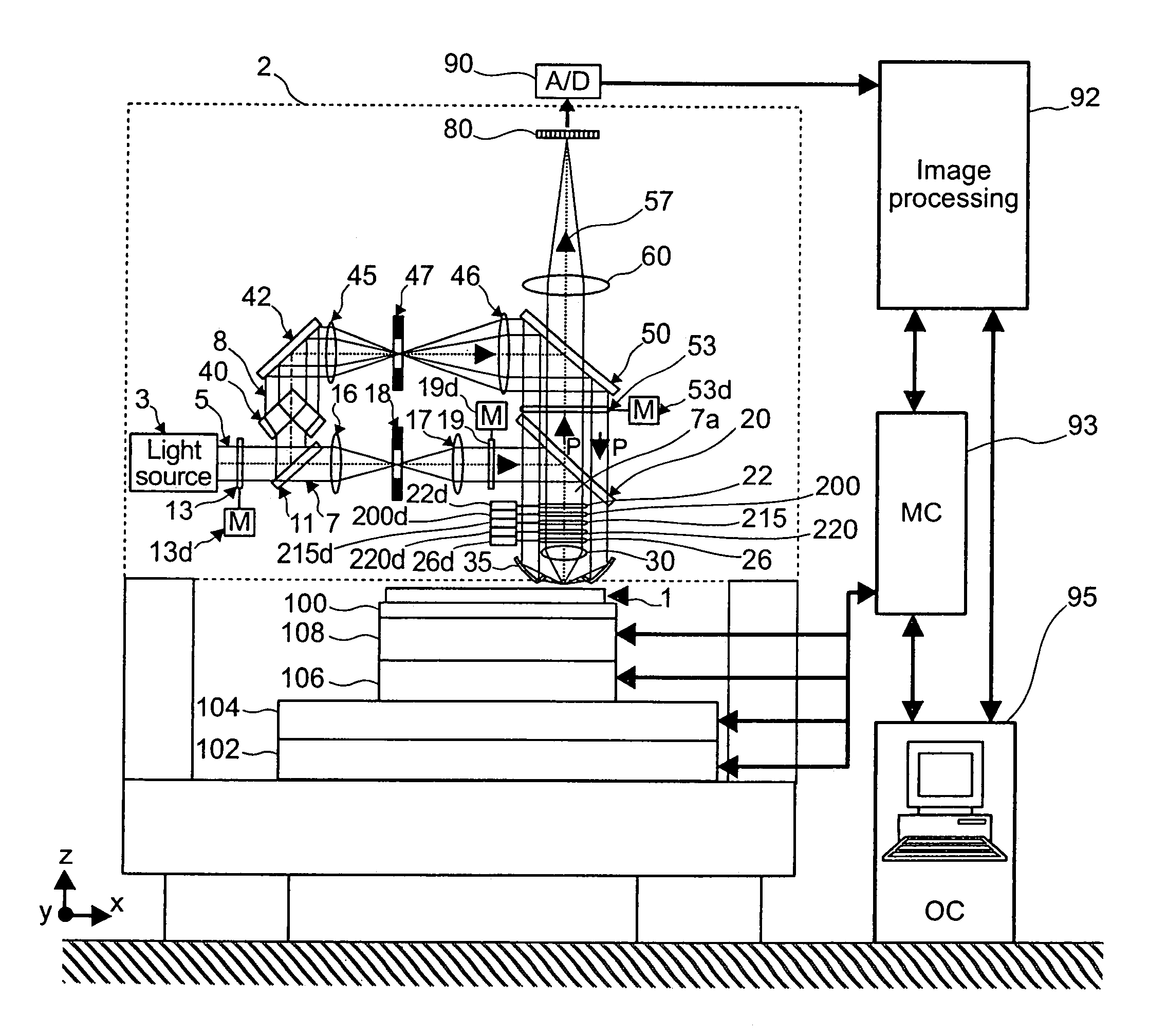
[0033]For example, an inspection process in the course of manufacture of semiconductor wafers is roughly classified into inspection of a transistor layer and inspection of a metal wiring layer. In the case of the transistor layer, fine irregularities of a formed pattern can constitute critical defects to a device, and an inspecting apparatus should detect those irregularities as defects. On the other hand, in the case of the metal wiring layer, since irregularities, such as grains, do not critically affect the device, they should not be detected. Accordingly, how irregularities affect a device determines whether the irregularities should be manifested or whether the contrast of them should be kept low. Therefore, in order to carry out an inspection process on semiconductor wafers with a single apparatus, the apparatus must be configured such that an optical condition to manifest irregularities and an optical condition to keep the contrast low can be set individually.
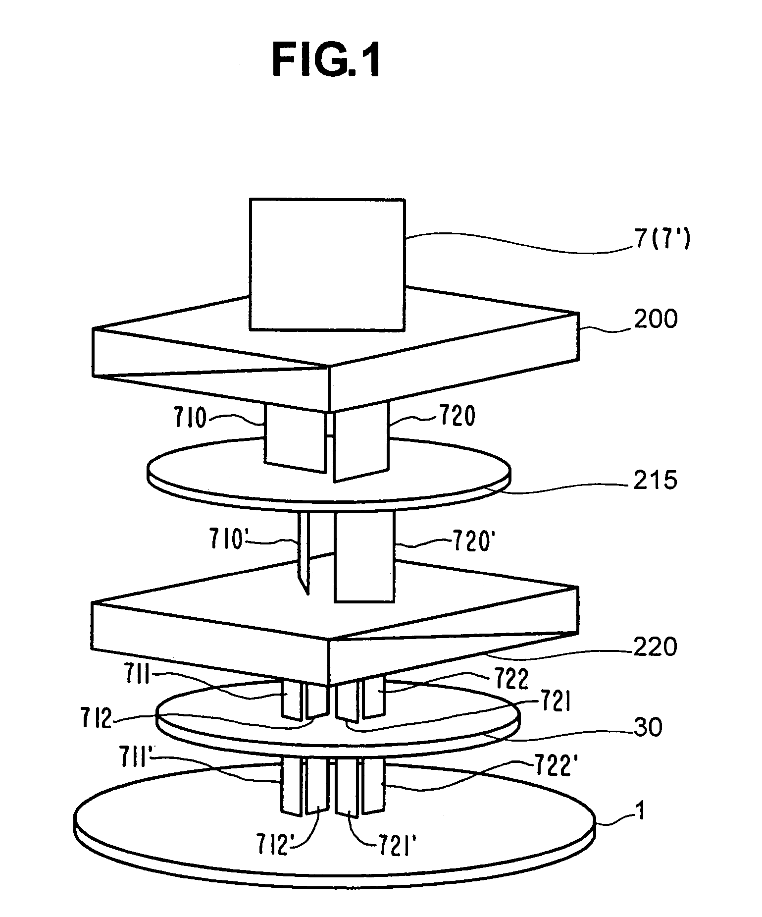
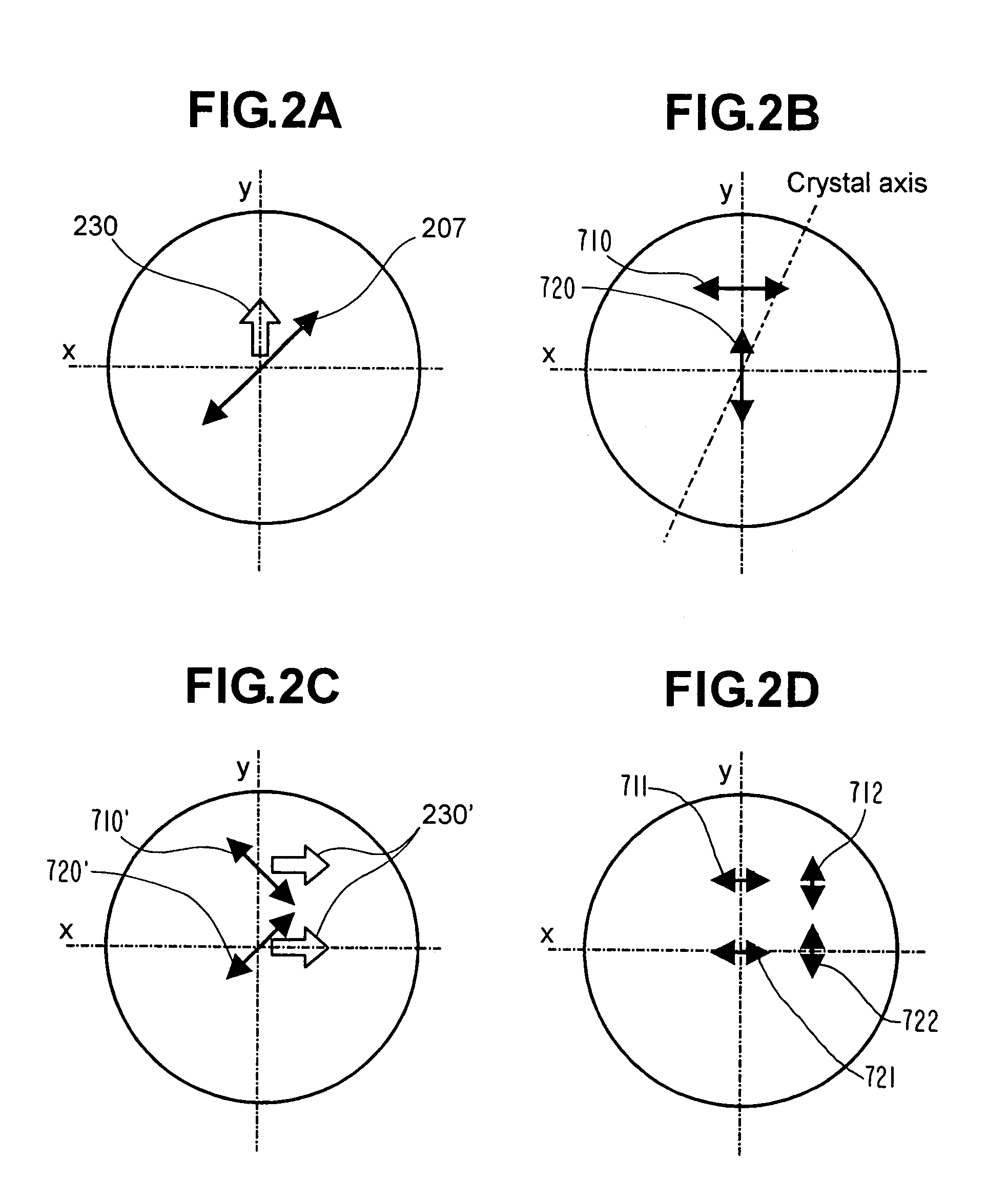
[0034]FIG. 1 sho...


PUM

PropertyMeasurementUnit
angleaaaaaaaaaa
angleaaaaaaaaaa
defectsaaaaaaaaaa

Abstract

Though it is necessary to enhance sensitivity in detecting defects as design rules grow finer, the resolution of a conventional optical system is not sufficient to cope with it. In order to increase vertical resolution, an optical system is so configured to perform detection by differential interference in which beams of light are sheared in two-dimensional directions in a plane perpendicular to an optical axis, thereby achieving zero-order light phase-difference detection. Further, the system is configured such that inconsistencies in brightness caused by thin-film interference, which appear as a noise component in a comparative inspection, are reduced by differential interference and dark-field illumination. Further, with respect to non-critical grains in metal wiring, the contrast of grains is reduced by bright-field/dark-field-combined illumination. The sensitivity in defect detection can be enhanced and highly sensitive inspection can be achieved even when detecting objects of various types and processes.

Description

BACKGROUND OF THE INVENTION[0001]The present invention relates to an optical system of the type used for inspection and observation of defects and foreign substance-induced defects in the surface of a pattern that is formed on a substrate through a thin film preparation process, such as a semiconductor production process and a flat-panel display manufacturing process. The invention also relates to a method of inspecting for defects using the optical system, an apparatus therefor, and a method for effectively using obtained inspection information.[0002]Japanese Patent Laid-Open No. 9-218165 discloses an optical system for inspecting photomasks. This optical system operates as a Mach-Zehnder interferometer in which two sheared beams of light are applied to a mask surface. Then, the two beams that have reflected off the mask are caused to interfere with each other so that an irregularity which constitutes a defect in the mask surface can be detected with a high sensitivity.[0003]In thi...

Claims


Application Information

Patent Timeline
Patent Type & Authority Patents(United States)
IPC IPC(8): G01N21/00G01B11/30G01M11/00G01N21/956
CPCG01N21/956
Inventor SHIBATA, YUKIHIROMAEDA, SHUNJIWATANABE, MASAHIRO
Owner HITACHI HIGH-TECH CORP
Why Eureka
Try Eureka