Field effect transistor (FET) having wire channels and method of fabricating the same

a field effect transistor and wire channel technology, applied in the direction of electrical equipment, semiconductor devices, radio frequency controlled devices, etc., can solve the problems of limited number of spaced channel layers in these conventional devices, and the ability of conventional devices to perform fast operations

Active Publication Date: 2007-09-25
SAMSUNG ELECTRONICS CO LTD
View PDF9 Cites 46 Cited by
  • Summary
  • Abstract
  • Description
  • Claims
  • Application Information

AI Technical Summary

Benefits of technology

[0007]It is a feature of an embodiment of the present invention to provide an FET having a plurality of wire channels and a method of fabricating the same that is able to prevent generation of a short channel effect and a narrow channel effect.
[0008]It is another feature of an embodiment of the present invention to provide an FET having a plurality of wire channels and a method of fabricating the same that is able to increase an operating speed of a corresponding semiconductor device.
[0009]It is still another feature of an embodiment of the present invention to provide an FET having a plurality of wire channels and a method of fabricating the same in which wire channels are completely surrounded by a gate electrode, which facilitates control of the channel by the gate electrode, thereby preventing a short channel effect and minimizing an inversion region formed on an exterior surface of the wire channel.
[0010]It is yet another feature of an embodiment of the present invention to provide an FET having a plurality of wire channels and a method of fabricating the same in which a width of the channel is increased to prevent a narrow channel effect.

Problems solved by technology

For example, these conventional devices are limited in an ability to perform fast operations.
Moreover, the number of spaced channel layers in these conventional devices is limited due to fabrication limitations, e.g., with respect to an etching depth that can be achieved during dry etching.

Method used


Image

  • Field effect transistor (FET) having wire channels and method of fabricating the same
  • Field effect transistor (FET) having wire channels and method of fabricating the same
  • Field effect transistor (FET) having wire channels and method of fabricating the same

Examples


Embodiment Construction

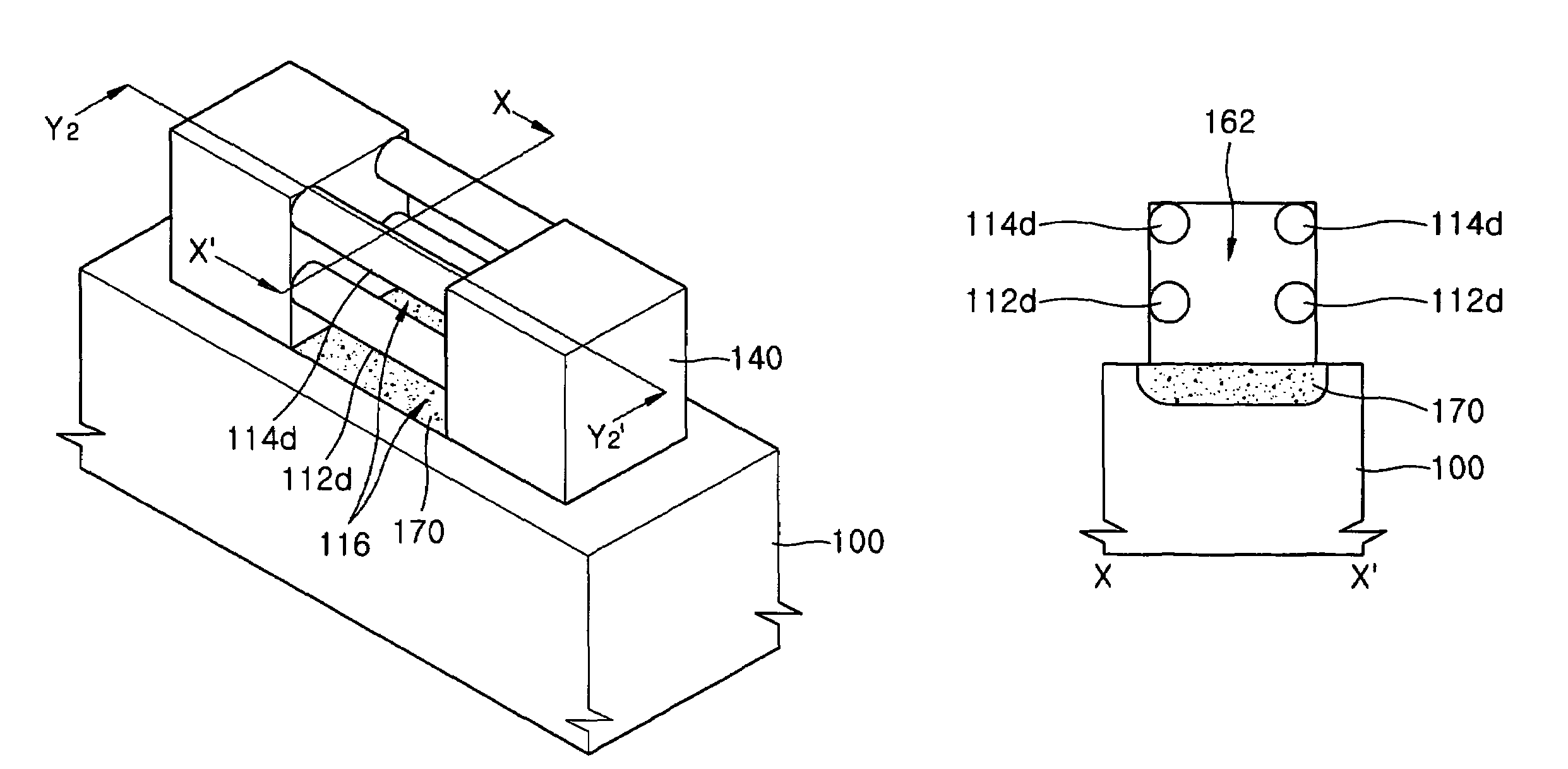
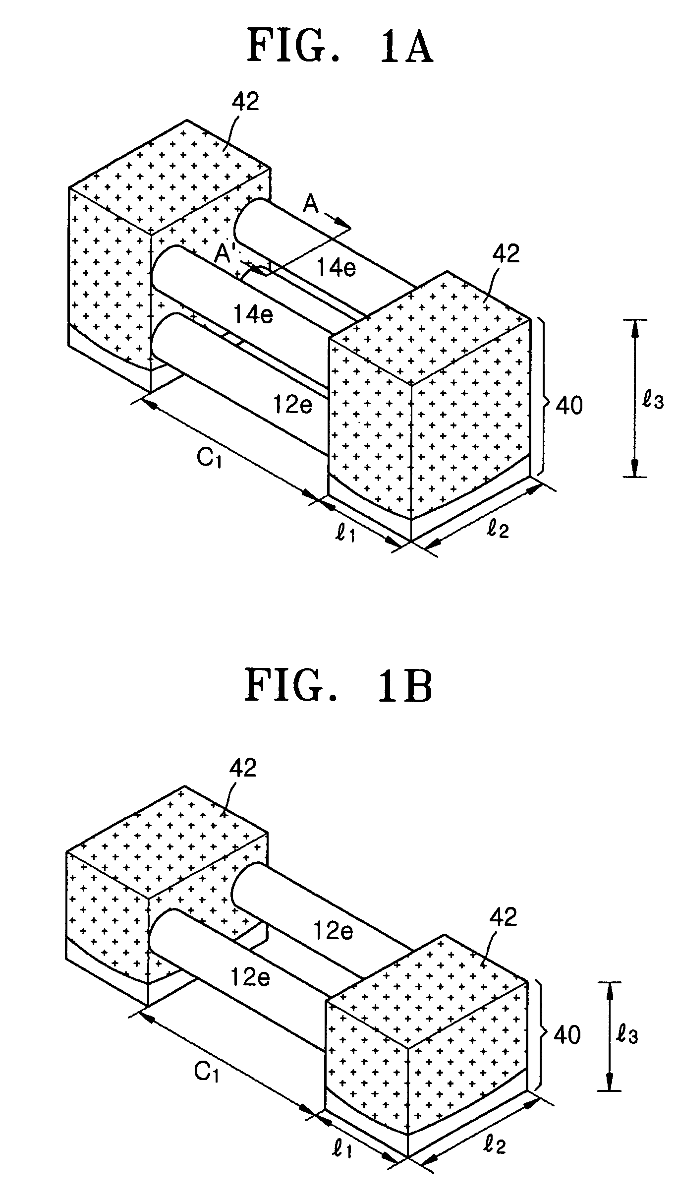
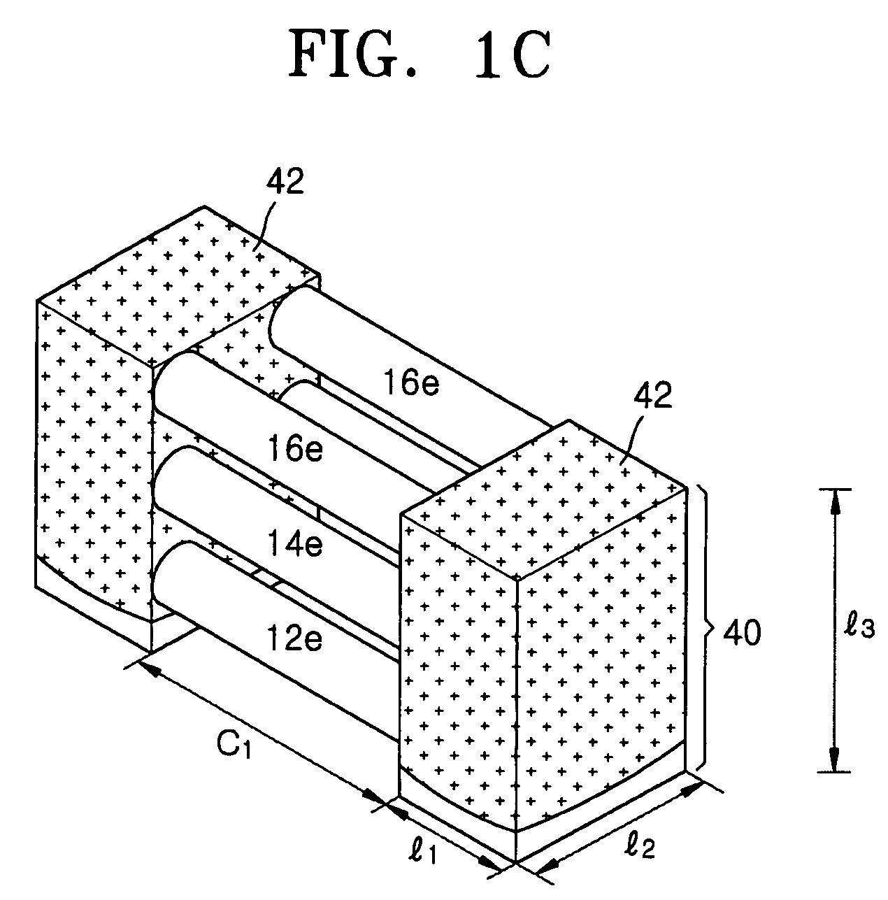
[0040]Korean Patent Application No. 2004-71225, filed on Sep. 7, 2004, in the Korean Intellectual Property Office, and entitled: “Metal-Oxide-Semiconductor Transistor Comprising Multiple Wire Bridge Channels and Method of Manufacturing the Metal-Oxide-Semiconductor Transistor,” is incorporated by reference herein in its entirety.

[0041]The present invention will now be described more fully hereinafter with reference to the accompanying drawings, in which exemplary embodiments of the invention are shown. The invention may, however, be embodied in different forms and should not be construed as limited to the embodiments set forth herein. Rather, these embodiments are provided so that this disclosure will be thorough and complete, and will fully convey the scope of the invention to those skilled in the art. In the drawings, the thickness of layers and regions are exaggerated for clarity. It will also be understood that when a layer is referred to as being “on” another layer or substrate...


PUM


Abstract

In a field effect transistor (FET), and a method of fabricating the same, the FET includes a semiconductor substrate, source and drain regions formed on the semiconductor substrate, a plurality of wire channels electrically connecting the source and drain regions, the plurality of wire channels being arranged in two columns and at least two rows, and a gate dielectric layer surrounding each of the plurality of wire channels and a gate electrode surrounding the gate dielectric layer and each of the plurality of wire channels.

Description

1. FIELD OF THE INVENTION[0001]The present invention relates to a field effect transistor (FET) and a method of fabricating the same. More particularly, the present invention relates to an FET having a plurality of wire channels and a method of fabricating the same.2. DESCRIPTION OF THE RELATED ART[0002]As applications of semiconductor devices expand, highly-integrated and / or high-speed semiconductor devices are increasingly in demand. As an integration density of semiconductor devices increase, a design rule becomes smaller. As a result of a decreasing design rule, a channel length and a channel width of a field effect transistor (FET) similarly decrease. A decrease in channel length may result in a short channel effect. A decrease in channel width may result in a narrow channel effect. The short channel effect may significantly influence a potential in a source / drain region upon a channel region. The narrow channel effect may increase a threshold voltage. In an attempt to prevent ...

Claims


Application Information

Patent Timeline
Patent Type & Authority Patents(United States)
IPC IPC(8): H01L29/76
CPCH01L29/42384H01L29/42392H01L29/78696H01L29/7854H01L29/78654H01L29/66772H01L29/41775H01L2224/4813
Inventor KIM, SUNGMINLI, MINGYOON, EUNGJUNG
Owner SAMSUNG ELECTRONICS CO LTD
Why Eureka
Try Eureka