

Organic electroluminescent device
an electroluminescent device and organic technology, applied in the direction of luminescnet screen, discharge tube luminescnet, natural mineral layered products, etc., can solve the problems of low reflectivity, low work function etc., to achieve enhanced optical efficiency and stability of organic el device, high work function, and high reflectivity
- Summary
- Abstract
- Description
- Claims
- Application Information
AI Technical Summary
Benefits of technology
Problems solved by technology
Method used
Image

Examples
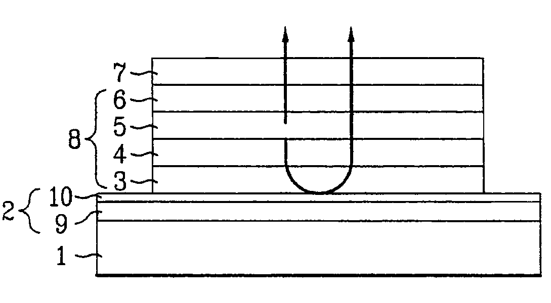
first embodiment
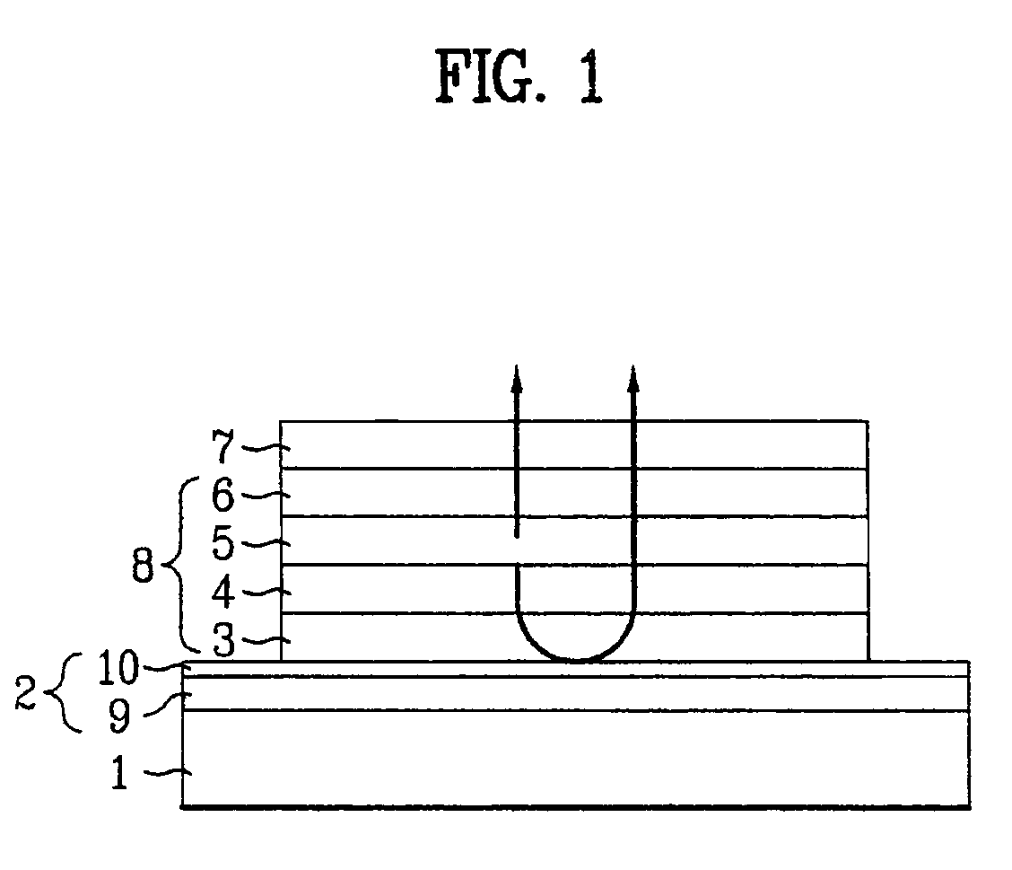
[0052]FIG. 2 is a graph of reflectivity variation depending on thickness of Cr layer on Al layer according to the present invention.
[0053]Referring to FIG. 2, the anode 2 includes the reflective layer 9 of Al and the hole injection layer 10 of Cr.
[0054]Al layer is deposited 150 nm thick using 4″ target of 99.999% at 200 W and 2 mTorr. Cr layers are deposited 2 nm, 3 nm, 7 nm, and 11 nm thick, respectively using 4″ target of 99.999% at 200 W and 1 mTorr.
[0055]As shown in the drawing, the more the thickness of Cr increases, the more overall reflectivity of the anode 2 decreases.
[0056]In case that the thickness of Cr exceeds 1 nm, the corresponding reflectivity is lower than reflectivity of the single Cr layer. Hence, it is unable to achieve the object of the present invention in improving the reflectivity.
[0057]By providing Cr with the thickness less than 10 nm, the reflectivity can be improved.
[0058]In doing so, if the deposition condition of Cr is varied to 10 mTorr, the correspondi...
second embodiment
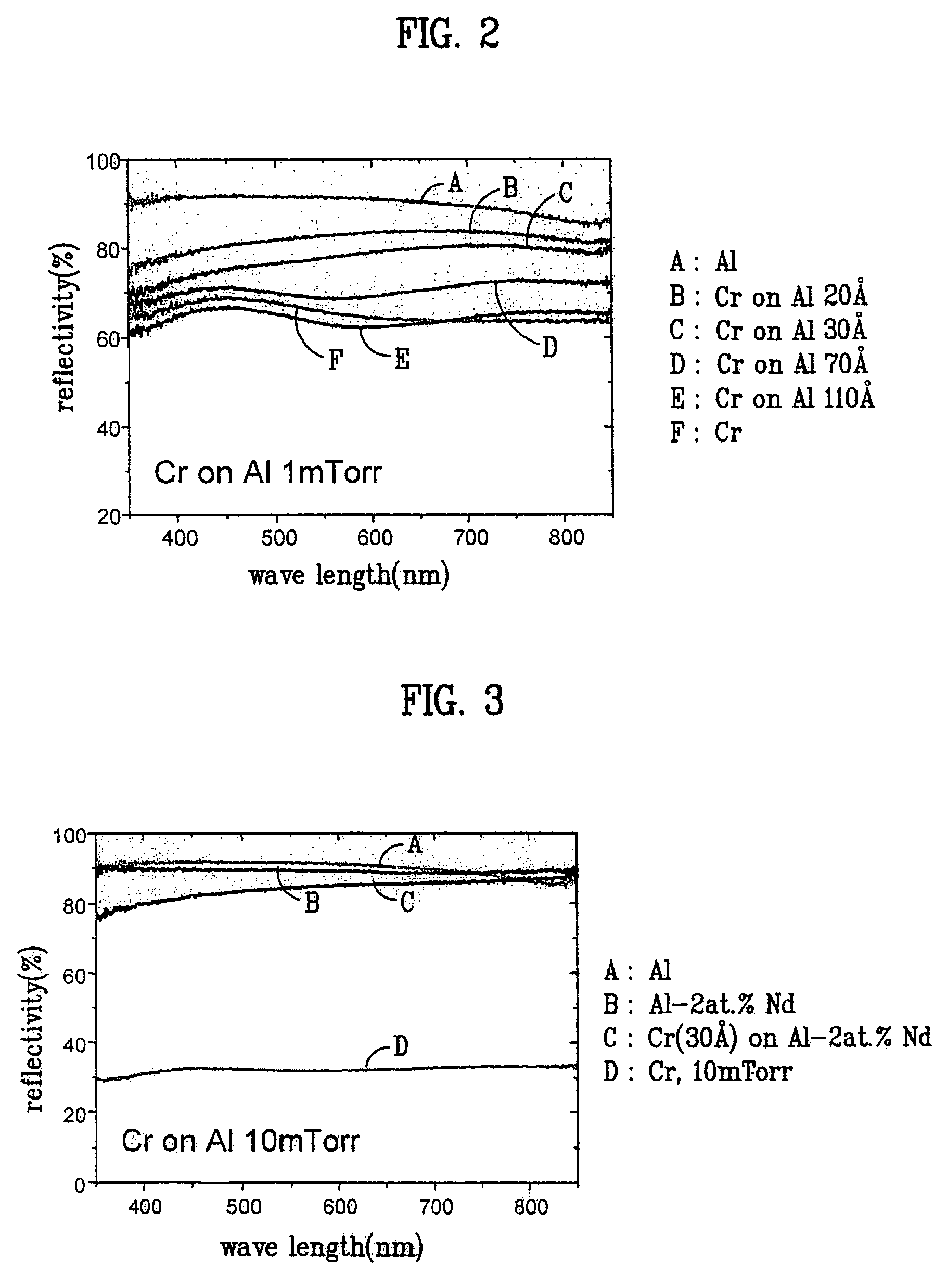
[0060]FIG. 3 is a graph of reflectivity variation depending on thickness of Cr layer on Al—Nd alloy reflective layer according to the present invention.
[0061]Referring to FIG. 3, instead of the Al layer, the reflective layer 9 for the anode 2 is formed 150 nm thick using 4″ Al-2 at. % Nd alloy target of 99.999% at 200 W and 1 mTorr.
[0062]And, a Cr layer as the hole injection layer 10 is formed 3 nm thick on the reflective layer 9 using 4″ target of 99.999% at 200 W and 10 mTorr.
[0063]Compared to the reflectivity of the case of the mono-atomic Al layer, reflectivity in the visible ray area is reduced about 2% in case of using the 2 at. % Nd-added Al target.
[0064]Yet, even if the Cr layer is deposited on the Al—Nd layer, it can be checked that there is almost no variation of the reflectivity of the Al—Nd layer.
[0065]Thus, if the alloy formed by adding one of Nd, Ta, Nb, Mo, W, Ti, Si, B, and Ni at about 5 at. % to Al is used as the reflective layer 9, reduction of the reflectivity alm...
PUM
| Property | Measurement | Unit |
|---|---|---|
| thick | aaaaa | aaaaa |
| reflectivity | aaaaa | aaaaa |
| wavelength range | aaaaa | aaaaa |
Abstract
Description
Claims
Application Information