Liquid crystal display device having touch screen function and method of fabricating the same

a technology of liquid crystal display device and touch screen, which is applied in the direction of identification means, instruments, computing, etc., can solve the problems of excessive flotation, inability to provide high-quality images, and lcd device in which a touch panel is attached to the liquid crystal panel

Active Publication Date: 2007-10-09
SAMSUNG DISPLAY CO LTD
View PDF13 Cites 151 Cited by
  • Summary
  • Abstract
  • Description
  • Claims
  • Application Information

AI Technical Summary

Benefits of technology

[0010]The present invention is conceived to solve the aforementioned problems. Accordingly, an object of the present invention is to provide an LCD device that can implement a touch screen function by constructing a circuit capable of reading variation in a liquid crystal cell gap without a need to separately attach a touch panel to the LCD device.

Problems solved by technology

However, the LCD device in which a touch panel is attached to the liquid crystal panel as mentioned above cannot provide high quality images, because the images are excessively floated due to light parallax occurring when light for displaying images reproduced on the liquid crystal panel is transmitted through the touch panel.
Therefore, there are problems in that it takes a lot of time to fabricate an LCD device while manufacturing costs also increase.

Method used


Image

  • Liquid crystal display device having touch screen function and method of fabricating the same
  • Liquid crystal display device having touch screen function and method of fabricating the same
  • Liquid crystal display device having touch screen function and method of fabricating the same

Examples


first embodiment

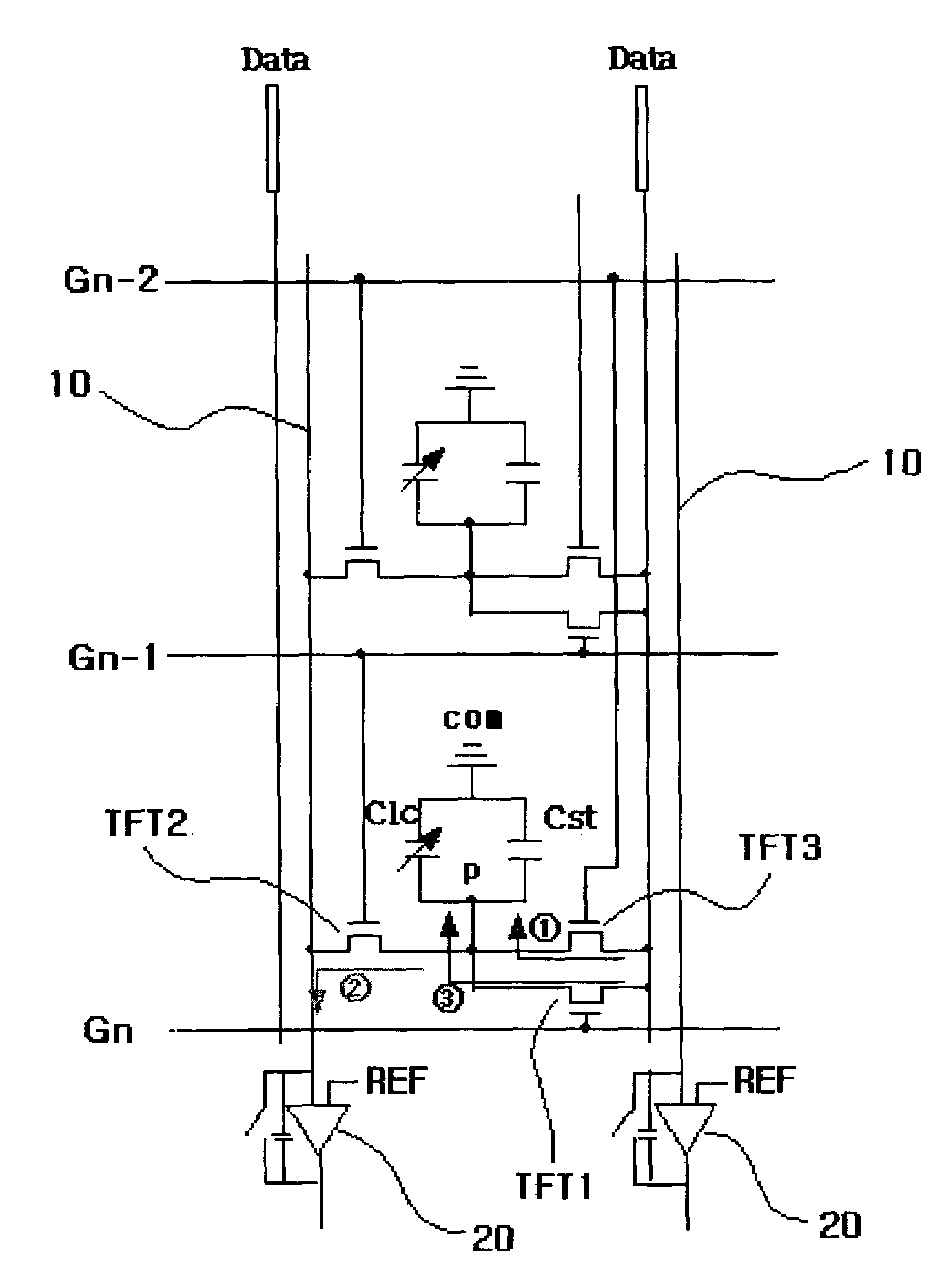
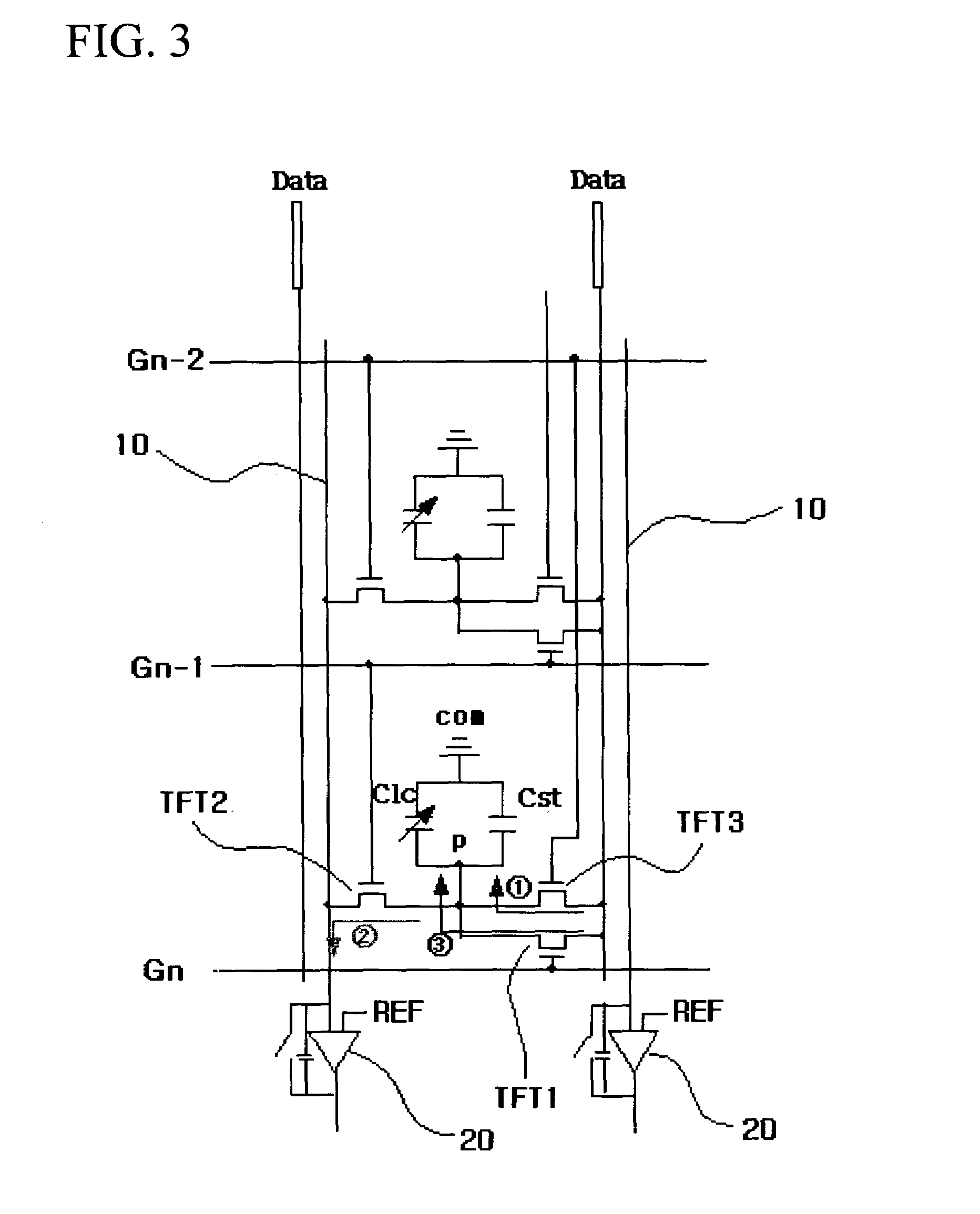
[0054]FIG. 3 is a circuit diagram illustrating the configuration of a liquid crystal display (LCD) device having a touch screen function according to the present invention.

[0055]As shown in FIG. 3, the LCD according to the first embodiment of the present invention includes a plurality of gate lines Gn, Gn-1, Gn-2, . . . that transfer scan signals, and a plurality of data lines Data that intersect the gate lines Gn, Gn-1, Gn-2, . . . and transfer image data.

[0056]Further, a plurality of signal lines 10 are insulated from and juxtaposed with the data lines Data.

[0057]First to third switching elements TFT1, TFT2 and TFT3 are formed in each of a plurality of pixel regions in the form of a matrix, which are surrounded by the gate lines Gn, Gn-1, Gn-2, . . . and the data lines Data. At this time, it is preferred that each of the switching elements be a thin film transistor.

[0058]Here, a gate electrode of the first switching element TFT1 is connected to the gate line Gn, a source electrode...

second embodiment

[0074]Next, an LCD device having a touch screen function according to the present invention will be described with reference to FIG. 4.

[0075]FIG. 4 is a circuit diagram illustrating the configuration of the LCD having the touch screen function according to the second embodiment of the present invention.

[0076]As shown in FIG. 4, the LCD device according to the second embodiment of the present invention includes a plurality of gate lines Gn, Gn-1, . . . , that transfer scan signals, and a plurality of data lines Data that intersect the gate lines Gn, Gn-1, . . . and transfer image data.

[0077]Further, a plurality of signal lines 10 are insulated from and juxtaposed with the data lines Data.

[0078]First and second switching elements TFT1 and TFT2 are formed in each of a plurality of pixel regions in the form of a matrix, which are surrounded by the gate lines Gn, Gn-1, . . . and the data lines Data. At this time, it is preferred that each of the two switching elements be a thin film tran...


PUM

PropertyMeasurementUnit
data voltageaaaaaaaaaa
voltageaaaaaaaaaa
capacitanceaaaaaaaaaa

Abstract

The present invention relates to an LCD device having a touch screen function. The LCD device of the present invention includes a plurality of gate lines, a plurality of data lines intersecting the gate lines, and a plurality of signal lines that are insulated from and juxtaposed with the data lines. First to third switching elements are formed in each of a plurality of pixel regions in the form of a matrix, which are surrounded by the gate lines and the data lines. Here, a gate electrode of the first switching element is connected to a gate line Gn, a source electrode thereof is connected to the data line, and a drain electrode thereof is connected to a pixel electrode. Further, liquid crystal capacitance and storage capacitance are formed between the pixel electrode and a common electrode. At this time, the liquid crystal capacitance is changed due to variation in the liquid crystal cell gap. The second and third switching elements are designed to read variation in the liquid crystal capacitance. A source electrode of the second switching element is connected to the pixel electrode, a drain electrode thereof is connected to the signal line, and a gate electrode thereof is connected to a previous gate line Gn-1. Furthermore, a source electrode of the third switching element is connected to the data line, a drain electrode thereof is connected to the pixel electrode, and a gate electrode thereof is connected to a second previous gate line Gn-2. Each signal line is connected to each signal amplifier.

Description

BACKGROUND OF THE INVENTION[0001]This application claims the priority of Korean Patent Application No. 10-2003-0077574 filed on Nov. 4, 2003 in the Korean Intellectual Property Office, the disclosure of which is incorporated herein by reference.[0002]1. Field of the Invention[0003]The present invention relates to a liquid crystal display device having a touch screen function. More particularly, the present invention is directed to a liquid crystal display device that is constructed to have a touch screen function using variation in liquid crystal cell capacitance due to variation in liquid crystal cell gaps.[0004]2. Description of the Related Art[0005]Generally, a liquid crystal display device is a display device for obtaining desired image signals by applying an electric field to a liquid crystal material that fills a gap between two substrates and has an anisotropic dielectric constant and controlling the intensity of the electric field, thereby adjusting the amount of light that ...

Claims


Application Information

Patent Timeline
Patent Type & Authority Patents(United States)
IPC IPC(8): G02F1/1335G02F1/133G02F1/1333G02F1/1362G02F1/1368G06F3/041G09F9/30
CPCG06F3/0412G02F1/13624G02F1/13338G02F1/133371G06F3/0447G02F1/133
Inventor CHOI, JOON-HOOJOO, IN-SOO
Owner SAMSUNG DISPLAY CO LTD
Why Eureka
Try Eureka