Apparatus and methods for detection of systematic defects

a technology of systematic defects and apparatus, applied in the direction of instruments, digital data processing details, computation using non-denominational number representations, etc., can solve the problem of increasing yield losses, chip electrical defects, and difficult identification of systematic failure locations in poorly yielding designs

Active Publication Date: 2007-10-09
KLA TENCOR TECH CORP
View PDF24 Cites 117 Cited by
  • Summary
  • Abstract
  • Description
  • Claims
  • Application Information

AI Technical Summary

Problems solved by technology

As feature sizes shrink in the deep sub-micron region, more and more yield losses are ascribed to complex interactions between design and manufacturing, and not just random defects.
Typical of such interactions are those where mask patterns do not faithfully reproduce themselves on the wafer and thereby make the chip prone to electrical defects.
Identifying the location of systematic failures in poorly yielding designs is very difficult.
However, finding the design locations where the unique nature of the layout made it prone to poor reproduction during lithography is still not possible.
In operation (e), it is determined whether a product structure that is fabricated based on a pattern representation similar to the second test structure representation is susceptible to systematic failure based on the plurality of simulated final resist patterns of the second test structure representation.
Finally, the product structure is defined as being susceptible to systematic failure when the simulated final resist pattern of one of the identified edge segment representations has a shift that is greater than the predetermined threshold.
When there is an unexpected voltage potential within a particular random test structure, it is determined that there is a defect within such particular random test structure.

Method used


Image

  • Apparatus and methods for detection of systematic defects
  • Apparatus and methods for detection of systematic defects
  • Apparatus and methods for detection of systematic defects

Examples


Embodiment Construction

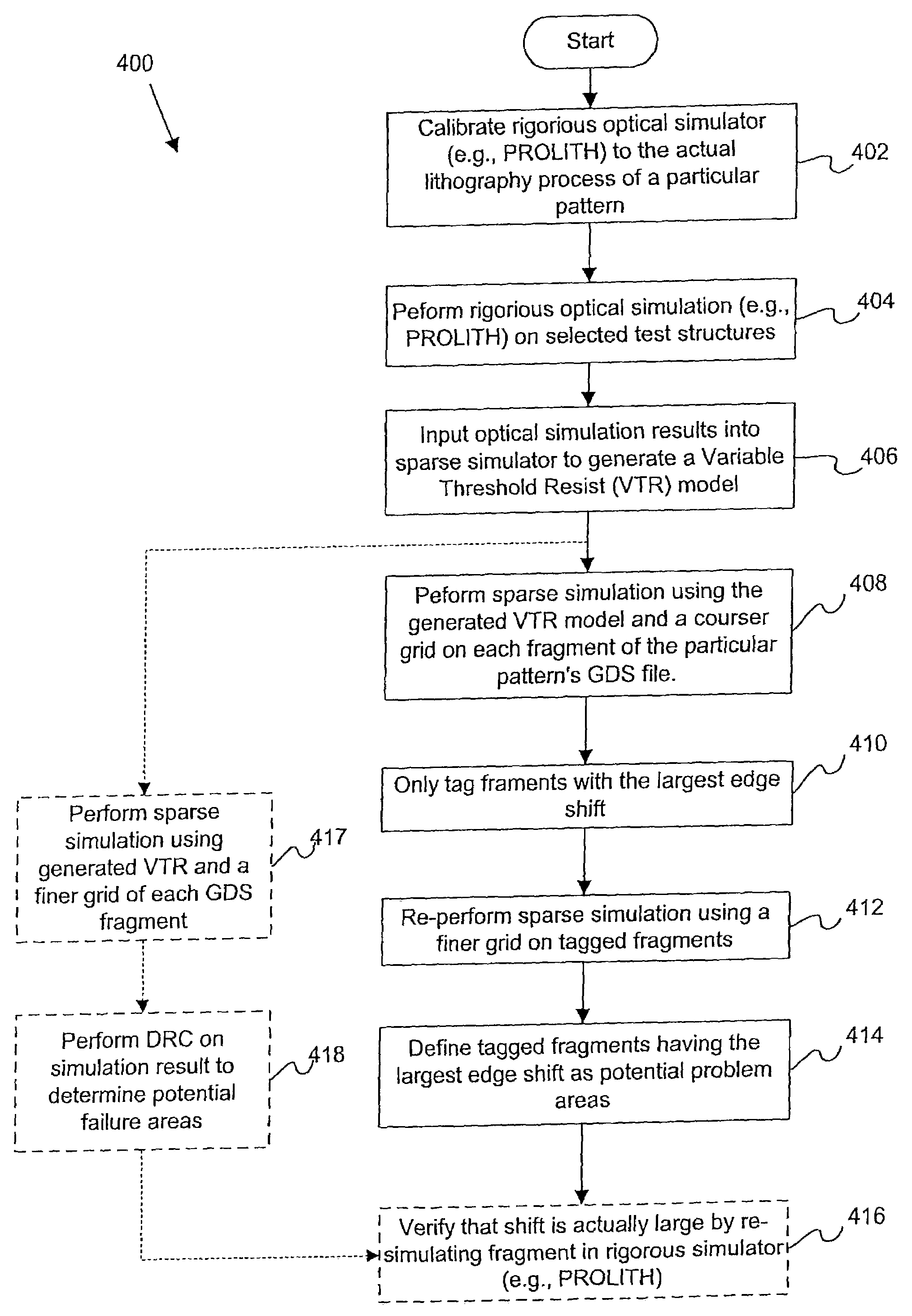
[0029]Reference will now be made in detail to a specific embodiment of the invention. An example of this embodiment is illustrated in the accompanying drawings. While the invention will be described in conjunction with this specific embodiment, it will be understood that it is not intended to limit the invention to one embodiment. On the contrary, it is intended to cover alternatives, modifications, and equivalents as may be included within the spirit and scope of the invention as defined by the appended claims. In the following description, numerous specific details are set forth in order to provide a thorough understanding of the present invention. The present invention may be practiced without some or all of these specific details. In other instances, well known process operations have not been described in detail in order not to unnecessarily obscure the present invention.

[0030]In general terms, specific semiconductor patterns that are susceptible to systematic defects are utili...


PUM


Abstract

Disclosed are mechanisms are provided for determining whether a particular integrated circuit (IC) pattern is susceptible to systematic failure, e.g., due to process fluctuations. In one embodiment, final resist patterns for such IC pattern are simulated using a sparse type simulator under various process settings. The sparse type simulator uses a model (e.g., a variable threshold resist model) for a particular photolithography process in which the IC pattern is to be fabricated. The model is generated from measurements taken from a plurality of simulated structures output from a rigorous type simulator. The simulated final resist patterns may then be analyzed to determine whether the corresponding IC pattern is susceptible to systematic failure. After an IC pattern which is susceptible to systematic failure has been found, a test structure may be fabricated from a plurality of IC patterns or cells. The cells of the test structure are arranged to have a particular pattern of voltage potential or brightness levels during a voltage contrast inspection. Mechanisms for quickly inspecting such test structures to thereby predict systematic yield of a product device containing patterns similar to the test structure cells are also disclosed.

Description

CROSS REFERENCE TO RELATED APPLICATIONS[0001]This application is a continuation-in-part and claims priority of U.S. patent application Ser. No. 09 / 991,188, which is now U.S. Pat. No. 6,732,002 issued 4 May 2004, entitled APPARATUS AND METHODS FOR PREDICTING MULTIPLE PRODUCT CHIP YIELDS THROUGH CRITICAL AREA MATCHING, filed 14 Nov. 2001, by Kurt H. Weiner et al, which patent is incorporated herein by reference in its entirety for all purposes.[0002]This application also claims priority of the U.S. Provisional Application, having an application No. 60 / 329,806, entitled APPARATUS AND METHODS FOR DETECTION OF SYSTEMATIC DEFECTS, filed 17 Oct. 2001, by Kurt H. Weiner et al., which application is incorporated herein by reference in its entirety for all purposes.BACKGROUND OF THE INVENTION[0003]This invention relates to methods and apparatus for detecting defects in a semiconductor test structure to thereby predict product yield.[0004]As feature sizes shrink in the deep sub-micron region, ...

Claims


Application Information

Patent Timeline
Patent Type & Authority Patents(United States)
IPC IPC(8): G06F17/10G06F17/50
CPCG01R31/318364
Inventor WEINER, KURT H.VERMA, GAURAVDE, INDRANIL
Owner KLA TENCOR TECH CORP
Why Eureka
Try Eureka