Surface mount type semiconductor device and lead frame structure thereof

a semiconductor device and lead frame technology, applied in semiconductor devices, semiconductor/solid-state device details, electrical devices, etc., can solve problems such as cracking or otherwise damaging the lamphouse, and achieve the effects of boosting the volume, reducing the area, and ensuring the effect of stability

Active Publication Date: 2007-10-16
STANLEY ELECTRIC CO LTD
View PDF25 Cites 78 Cited by
  • Summary
  • Abstract
  • Description
  • Claims
  • Application Information

AI Technical Summary

Benefits of technology

[0019]In accordance with one of several aspects of the present invention, a simple configuration is provided for a surface mount type semiconductor device and lead frame structure thereof for, among other reasons, improving the heat radiating property of the lead frames and reducing stress during forming of the lead frames. The surface mount type semiconductor device can include a pair of lead frames that are butted to each other with a spacing such that one end of the lead frames are opposite to each other. A bare chip can be mounted on a chip mount portion on one end side of one of the lead frames and wire-bonded to a connection portion on one end side of the other lead frame. A housing is preferably insert-molded to one end sides of both of the lead frames. The lead frames can be shaped by forming so as to extend along the side and bottom surfaces of the housing and to form surface mounting terminal portions. The lead frames are also preferably formed such that they are thin at least at the regions to be bent during forming, with other regions thereof formed to be thick to improve heat radiating effect.
[0021]According to another aspect of the present invention a lead frame structure of a surface mount type semiconductor device can include a pair of lead frames that are butted to each other with a spacing such that one end of the lead frames are opposite to each other. A bare chip can be mounted on a chip mount portion on one end side of one of the lead frames and wire-bonded to a connection portion on one end side of the other lead frame. A housing can be insert-molded to one end side of both of the lead frames, wherein the lead frames can be shaped by forming so as to extend along the side and bottom surfaces of the housing and to form surface mounting terminal portions. The lead frames are preferably formed such that they are thin at least at the regions to be bent during forming, with other regions thereof formed such that they are thick to improve heat radiating effect.
[0023]The exposed portions on the side and bottom surfaces of the housing of the lead frames can be connected to the connection land on the mount substrate by surface mounting the semiconductor device. The bare chip can be powered from both lead frames, thus putting the bare chip into operation.
[0024]In this case, the individual lead frames can be formed to be thick as a whole, thus boosting their volumes. This can secure a sufficient volume for the individual lead frames even if the semiconductor package is small in size, and therefore the lead frames can be relatively small in area. This can lead to improvements in heat radiating effect of the lead frames, thus efficiently radiating heat generated during the operation of the bare chip mounted on the chip mount portion of one of the lead frames.
[0025]The lead frames can be thinly formed at the regions that are to be bent during forming, keeping stress that occurs during forming relatively small and considerably reducing the likelihood of cracking or otherwise damaging the housing that is molded to the lead frames.
[0026]If the lead frames are thinly formed at the regions of the mutually-opposing end surfaces on the rear surface side and, more specifically, if the lead frames are provided with stepped or sloped portions at the regions of the mutually-opposing end surfaces on the rear surface, the butt thickness of the lead frames at the mutually-opposing end surfaces will diminish. Thus, it is possible, even when a spacing that is wider than the butt thickness is secured, to reduce the spacing between the mutually-opposing end surfaces of the lead frames and further downsize the package of the surface mount type semiconductor device. Thus, the lead frames can be formed to be thick as a whole, boosting the volumes of the lead frames and improving their heat radiating property.

Problems solved by technology

However, increasing the thicknesses of the lead frames 2 and 3 leads to a relatively large stress acting on the lamphouse 5 during forming of the lead frames 2 and 3, which can possibly crack or otherwise damage the lamphouse 5 under certain circumstances.
The same problems are apparent in other surface mount type semiconductor devices such as devices that generate heat during operation, namely, semiconductor laser devices, various ICs, etc.

Method used


Image

  • Surface mount type semiconductor device and lead frame structure thereof
  • Surface mount type semiconductor device and lead frame structure thereof
  • Surface mount type semiconductor device and lead frame structure thereof

Examples


Embodiment Construction

[0037]Preferred embodiments of the present invention will be described below in detail with reference to FIGS. 1 to 3.

[0038]It is to be noted that while the embodiments described below are preferred specific examples of the present invention and therefore have various technically preferred features, the present invention is not limited thereto.

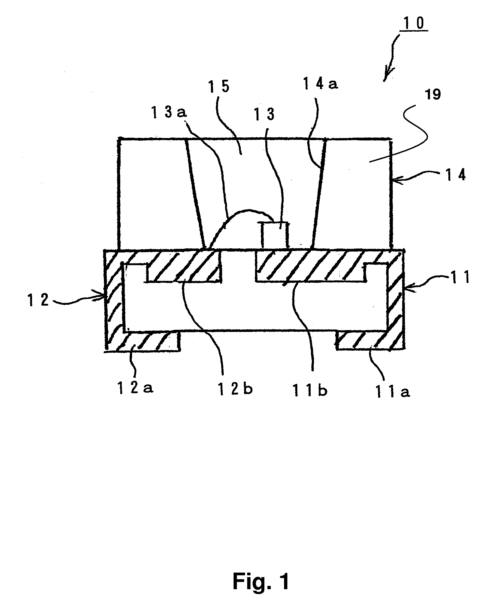
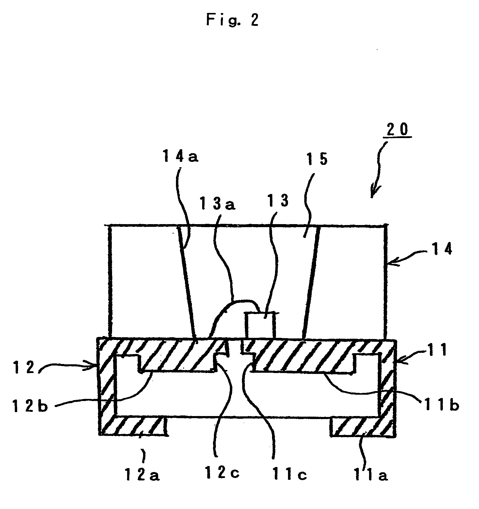
[0039]FIGS. 1 to 3 show the configuration of various embodiments of a surface mount type LED made in accordance with the principle of the present invention.

[0040]In FIG. 1, a surface mount type LED 10 can include a pair of lead frames 11 and 12, an LED chip 13 mounted on the lead frame 11, a hollow lamphouse 14 configured as a housing 19 that is preferably insert-molded to the lead frames 11 and 12. A sealing resin 15 can be filled into a hollow portion 14a of the lamphouse 14.

[0041]The lead frames 11 and 12, can each be made of a conductive material such as iron- or copper-based metal, and can be provided with surface mounting terminal portio...


PUM


Abstract

A surface mount type semiconductor device can be configured to include a pair of lead frames that are butted to each other with a spacing such that ends of the lead frames are opposite to each other. A bare chip can be mounted on a chip mount portion on one end side of one of the lead frames, and wire-bonded to a connection portion on an end side of the other lead frame. A housing can be insert-molded to an end side of both of the lead frames, and the lead frames can be shaped such that they extend along the side and bottom surfaces of the housing and form surface mounting terminal portions. The lead frames are preferably formed to be thin at least at the regions that are to be bent, and other regions thereof are preferably formed to be thick to improve heat radiating effect.

Description

[0001]This invention claims the benefit of Japanese patent application No. 2004-000042, filed on Jan. 5, 2004, which is hereby incorporated by reference.FIELD OF THE INVENTION[0002]The present invention relates to a surface mount type semiconductor device. More specifically, this invention relates to a surface mount type semiconductor device that can include a bare chip mounted on a lead frame arranged on a substrate, and to a lead frame structure thereof.DESCRIPTION OF THE RELATED ART[0003]A surface mount type semiconductor device such as a surface mount type LED has conventionally been configured as shown in FIGS. 4 to 6. In FIGS. 4 and 5, a surface mount type LED 1 includes a pair of lead frames 2 and 3, an LED chip 4 mounted on the lead frame 2, a hollow lamphouse 5 insert-molded to the lead frames 2 and 3 and a sealing resin 6 filled into a hollow portion 5a of the lamphouse 5.[0004]The lead frames 2 and 3, are each made of a conductive material such as iron- or copper-based me...

Claims


Application Information

Patent Timeline
Patent Type & Authority Patents(United States)
IPC IPC(8): H01L23/48H01L23/495H01L23/50H01L27/15H01L33/56H01L33/62H01L33/64
CPCH01L33/62H01L33/486H01L2224/48091H01L2224/48247H01L2924/01079H01L2924/12041H01L2224/45144H01L2924/00014
Inventor YOSHIDA, KENICHI
Owner STANLEY ELECTRIC CO LTD
Why Eureka
Try Eureka