Wireless device antenna

a technology of flex-rigid antennas and wireless devices, which is applied in the direction of resonant antennas, substantially flat resonant elements, and elongated active elements, etc., can solve the problems of flex-rigid technology, substantial increase in component parts,

Inactive Publication Date: 2007-10-30
NOKIA SOLUTIONS & NETWORKS OY
View PDF11 Cites 129 Cited by
  • Summary
  • Abstract
  • Description
  • Claims
  • Application Information

AI Technical Summary

Problems solved by technology

The number of supported systems directly increases the number of required antennas, which results in a substantial increase in the component part count.
However it is not known to use flex-rigid technology to integrate the antenna with the wireless device motherboard.

Method used


Image

  • Wireless device antenna
  • Wireless device antenna
  • Wireless device antenna

Examples


second embodiment

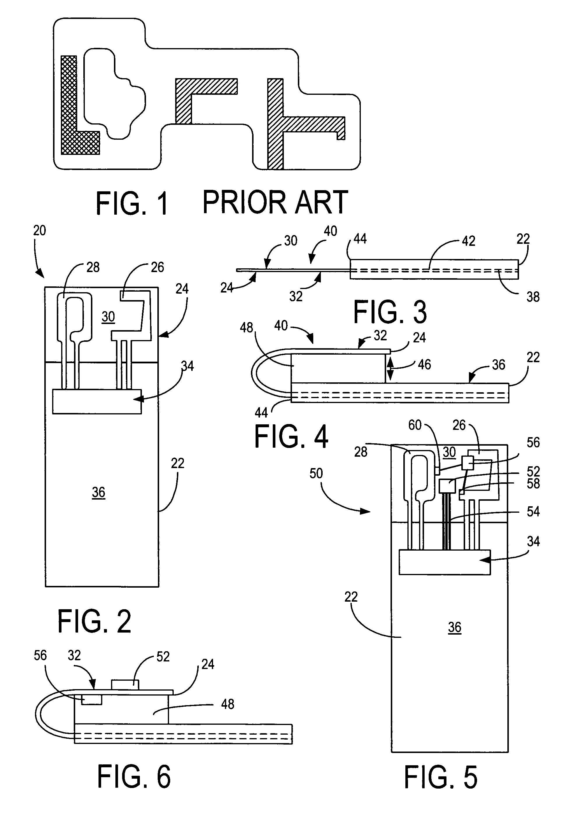
[0052]Referring now to FIGS. 5 and 6, a wireless device antenna generally designated 50 is illustrated therein in the invention wherein the second printed wiring board 24 is arranged to carry surface mount devices (SMD) which may be utilized, for example, tuning the radiating elements 26, 28 carried on the surface 30 of the second printed wiring board 24. In the illustrated embodiment, SMD 52 may carry control circuitry which is electrically connected to the RF transceiver 34 via leads 54 to receive the appropriate electronic control signals to adjust the tuning of the radiating elements 26, 28 by controlling the electronic tuning circuitry carried in the SMD 56 which is electrically connected to the radiating elements 26, 28 at points 58, 60 respectively to change the tuning characteristics of the radiating element pattern as well known and understood by those skilled in the art.

third embodiment

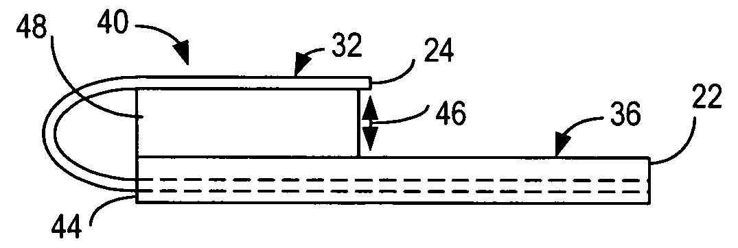
[0053]Turning now to FIGS. 7 and 8, the wireless device antenna is illustrated in a third embodiment and generally designated 70 and includes a first main printed wiring board 22 having a major surface 36 for carrying RF transceiver circuitry generally designated 34. The second printed wiring board generally designated 72 is rigid and manufactured and fabricated at the same time and as part of the same flex-rigid printed wiring board technology process as the main printed wiring board 22 and is flexibly connected to the first main printed wiring board by a flexible element generally designated 88. The flexible element 88 is defined by one or more dielectric layers 82 common to the first main printed wiring board 22 and the second printed wiring board 72 and which dielectric layers 82 extend continuously between the first main printed wiring board 22 and the second printed wiring board 72 such that the portion 90 of the dielectric layers 82 defines the flexible element 88 and permits...

fifth embodiment

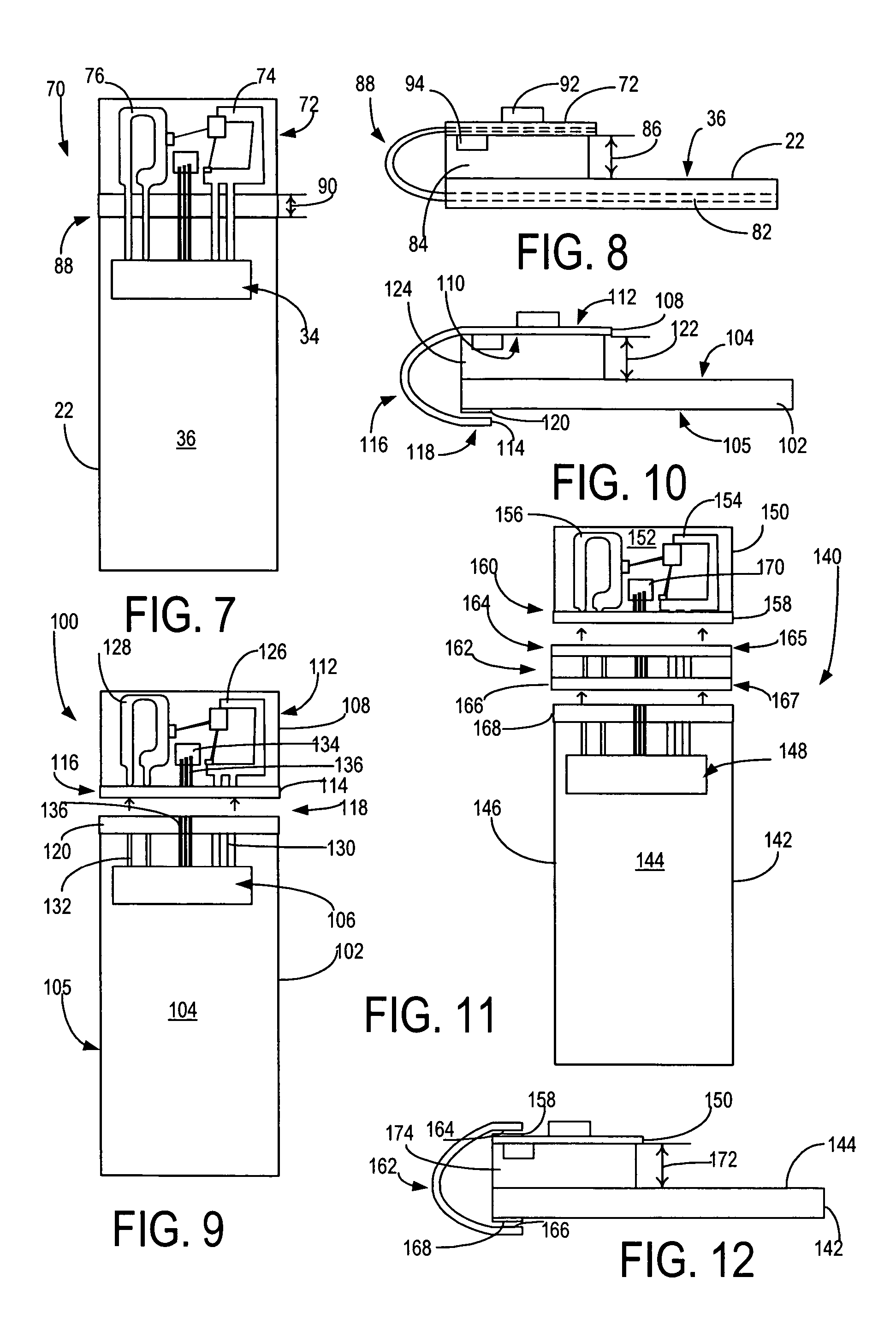
[0055]A wireless device antenna is illustrated in FIGS. 11 and 12 in the present invention and is generally designated 140 and includes a first main printed wiring board 142 flexibly coupled to a second printed wiring board 150 by a separate flexible element generally designated 162. The first main printed wiring board 142 includes a first major surface 144 for carrying RF transceiver circuitry 148 and an oppositely disposed second major surface 146. The second printed wiring board 150 includes a first major surface 152 for carrying radiating elements 154, 156. A connector 158 is defined at one end 160 of the flexible second printed wiring board 150. The flexible element 162 includes a connector 164 formed at one end 165 of the flexible element 162 for inter-engaging connection with the connector 158 of the second printed wiring board 150. A second connector 166 is arranged at the opposite end 167 of the flexible element 162 for inter-engagement connection with a connector 168 carri...


PUM


Abstract

A wireless device antenna is constructed using flex-rigid printed wiring board technology wherein a first main printed wiring board is flexibly connected to a second printed wiring board carrying at least one radiating element having an approximate length, width and pattern defining an intended antenna functionality which may be cellular, non-cellular or both. The first main printed wiring board and the second printed wiring board are flexibly and electrically connected to one another by a flexible element. An RF transmission line formed in the metallization layers common to the first main printed wiring board and the second printed wiring board connect transceiver circuitry carried on the first main printed wiring board to respective radiating elements carried on the second printed wiring board.

Description

FIELD OF THE INVENTION[0001]The present invention relates generally to wireless portable electronic devices for example, mobile telephones and deals more particularly with a wireless device integrated flex-rigid antenna. The invention more specifically deals with using flex-rigid printed wiring board (PWB) technology to integrate one or more antennas with the wireless device motherboard.BACKGROUND OF THE INVENTION[0002]The mobile wireless industry particularly the mobile telephone industry is under increasing pressure to bring products to market in shorter timeframes with increased performance and more features. This demand has forced designers to further integrate functions and reduce component part count and further concentrate on improved size reduction. One solution has been to use an internal antenna to provide cellular system, for example, GSM, WCDMA and non-cellular system, for example, Bluetooth, WLAN, BVB-H, UWB, FM-Radio communication functionality. The number of supported...

Claims


Application Information

Patent Timeline
Patent Type & Authority Patents(United States)
IPC IPC(8): H01Q1/24
CPCH01Q1/243H01Q1/38H01Q9/30H01Q9/0407H05K1/148H05K1/141
Inventor RANTA, TERO
Owner NOKIA SOLUTIONS & NETWORKS OY
Why Eureka
Try Eureka