
Method of testing semiconductor apparatus

a technology of semiconductor apparatus and test method, which is applied in the direction of recording signal processing, instruments, and recording information storage, etc., can solve the problem of not being able to guarantee a predetermined operation speed

Inactive Publication Date: 2007-10-30
SOCIONEXT INC
View PDF8 Cites 11 Cited by
  • Summary
  • Abstract
  • Description
  • Claims
  • Application Information

AI Technical Summary

Benefits of technology

The present invention provides a method for testing a semiconductor apparatus that can accurately screen it through a delay test even if the actual chip has different critical paths due to process variation. The method involves dividing the chip into multiple regions and extracting all paths that connect registers as candidate paths. The critical path is then selected based on process information of each region and a delay test is conducted for each region. This method allows for more efficient screening of semiconductor apparatus and ensures accurate testing of the critical path.

Problems solved by technology

As a result, a path having an increased delay time in a signal transmission than an initially assumed critical path is generated, resulting in a failure to guarantee a predetermined operation speed.

Method used


Image

  • Method of testing semiconductor apparatus
  • Method of testing semiconductor apparatus
  • Method of testing semiconductor apparatus

Examples


embodiment 1

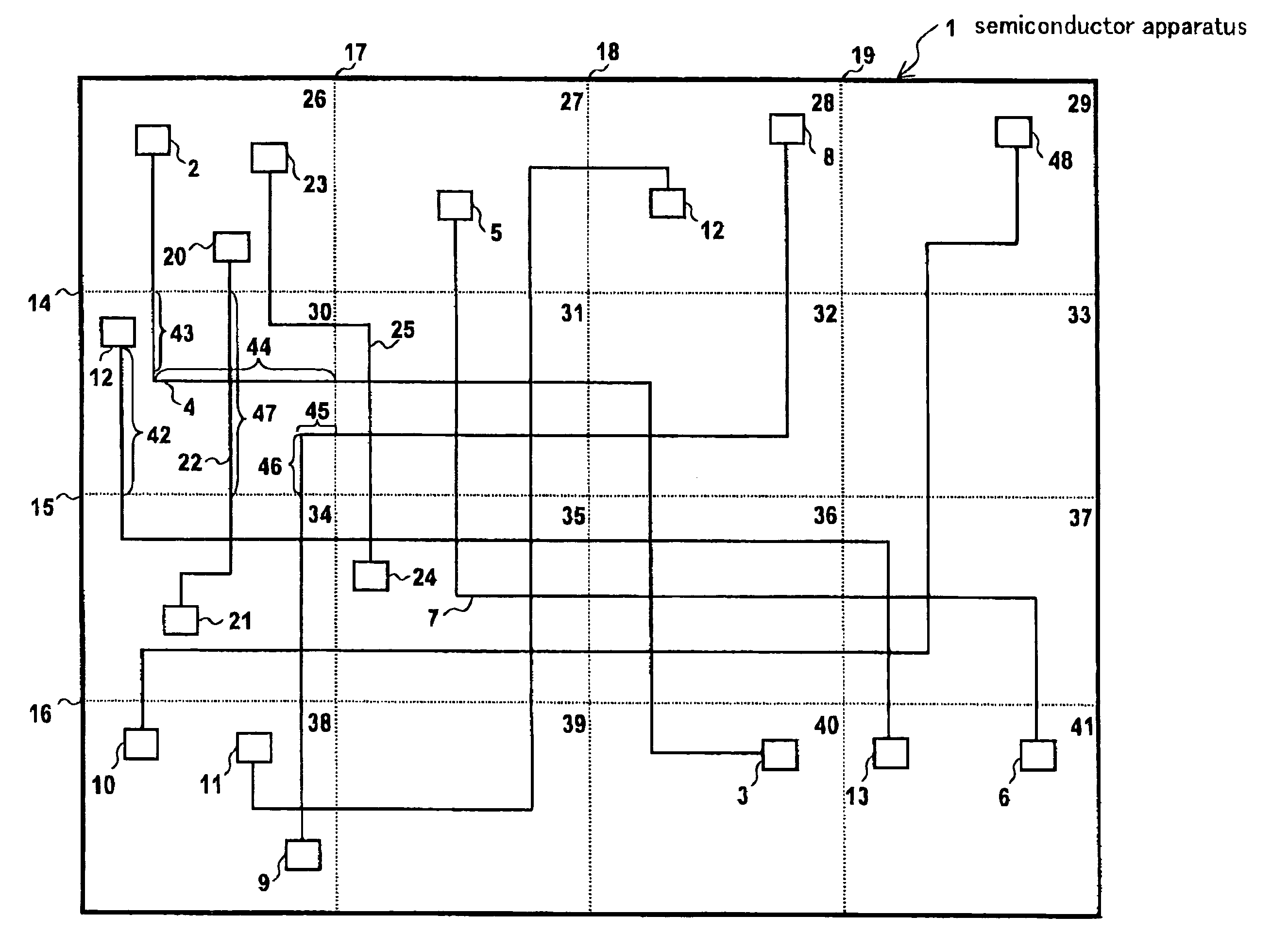
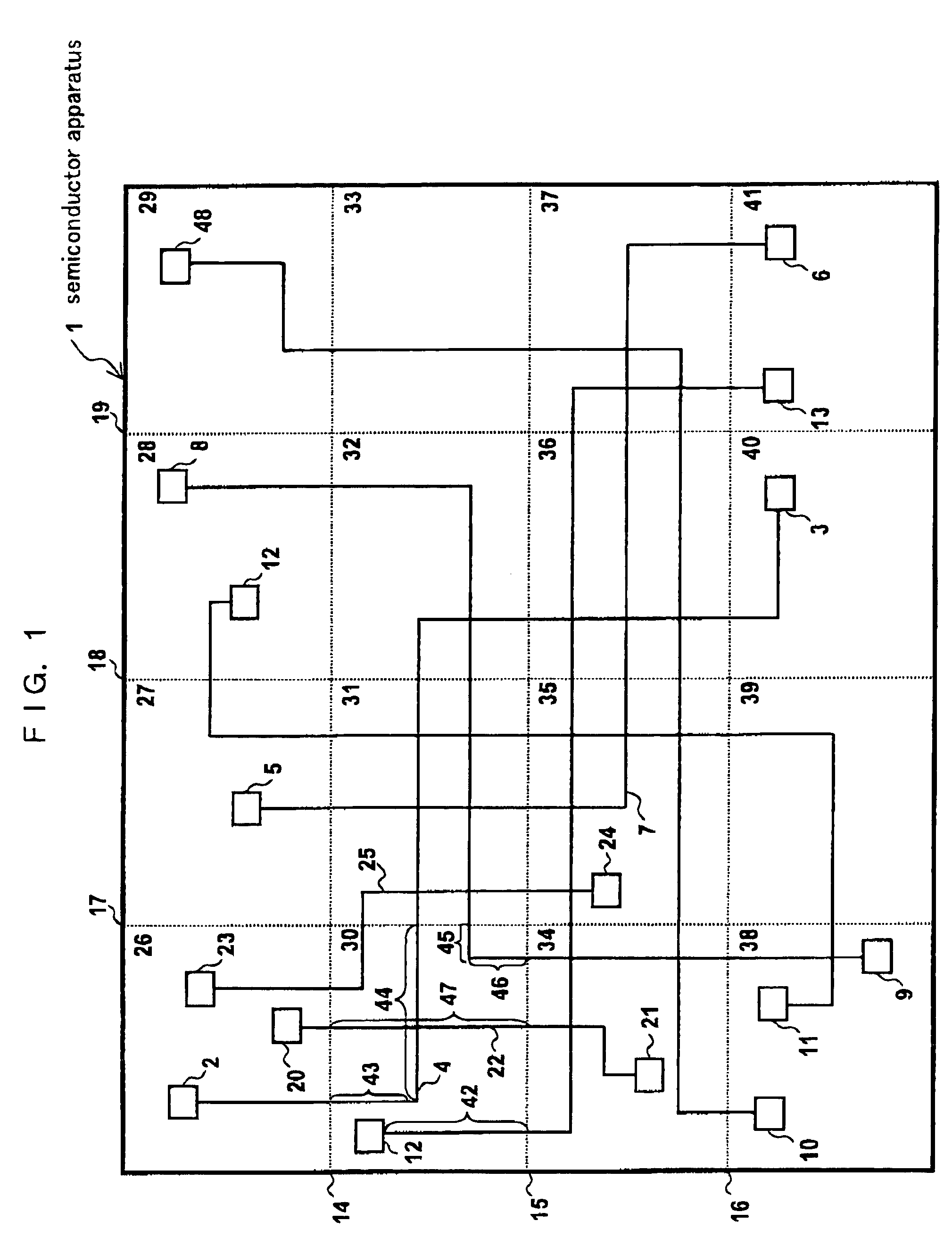
[0086]FIG. 1 shows a semiconductor apparatus according to an embodiment 1. A semiconductor apparatus 1 is divided by horizontal division lines 14, 15 and 16 and vertical division lines 17, 18 and 19 to thereby create divided regions 26-41. The divided region 26 includes registers 2, 20 and 23. The divided region 27 includes a register 5. The other divided regions also include registers.

[0087]Steps of the method of testing the semiconductor apparatus are as follows,[0088]1) The semiconductor apparatus 1 is divided into a plurality of divided regions as described.[0089]2) The registers present in the respective divided regions are extracted based on coordinates of the divided regions and registers.[0090]3) All of paths routed from the extracted registers to other registers are extracted as candidate paths. The candidate paths are comprised of wirings and logic gates.[0091]4) Concerning the plurality of extracted paths, delay times in signal transmissions are calculated based on arrang...

embodiment 2

[0101]An embodiment 2 is further described referring to FIG. 1.

[0102]Referring to the divided region 30, wiring paths 42, 43, 44, 45, 46 and 47 are extracted.

[0103]Steps of the method of testing the semiconductor apparatus are as follows.[0104]1) The semiconductor apparatus 1 is divided into a plurality of divided regions as described.[0105]2) All of wiring paths in the divided regions are extracted.[0106]3) Paths routed from registers to the registers by way of the respective extracted wiring paths are selected as candidate paths.[0107]4) Delay times in the plurality of candidate paths are compared to each other to thereby select the candidate path having a maximum delay time is selected as a critical path.[0108]5) A delay test is conducted for the critical path. More specifically, the initialization pattern is set in the critical paths selected in the respective divided regions, and the critical path is operated. Next, the transition pattern is set therein, and the critical path i...

embodiment 3

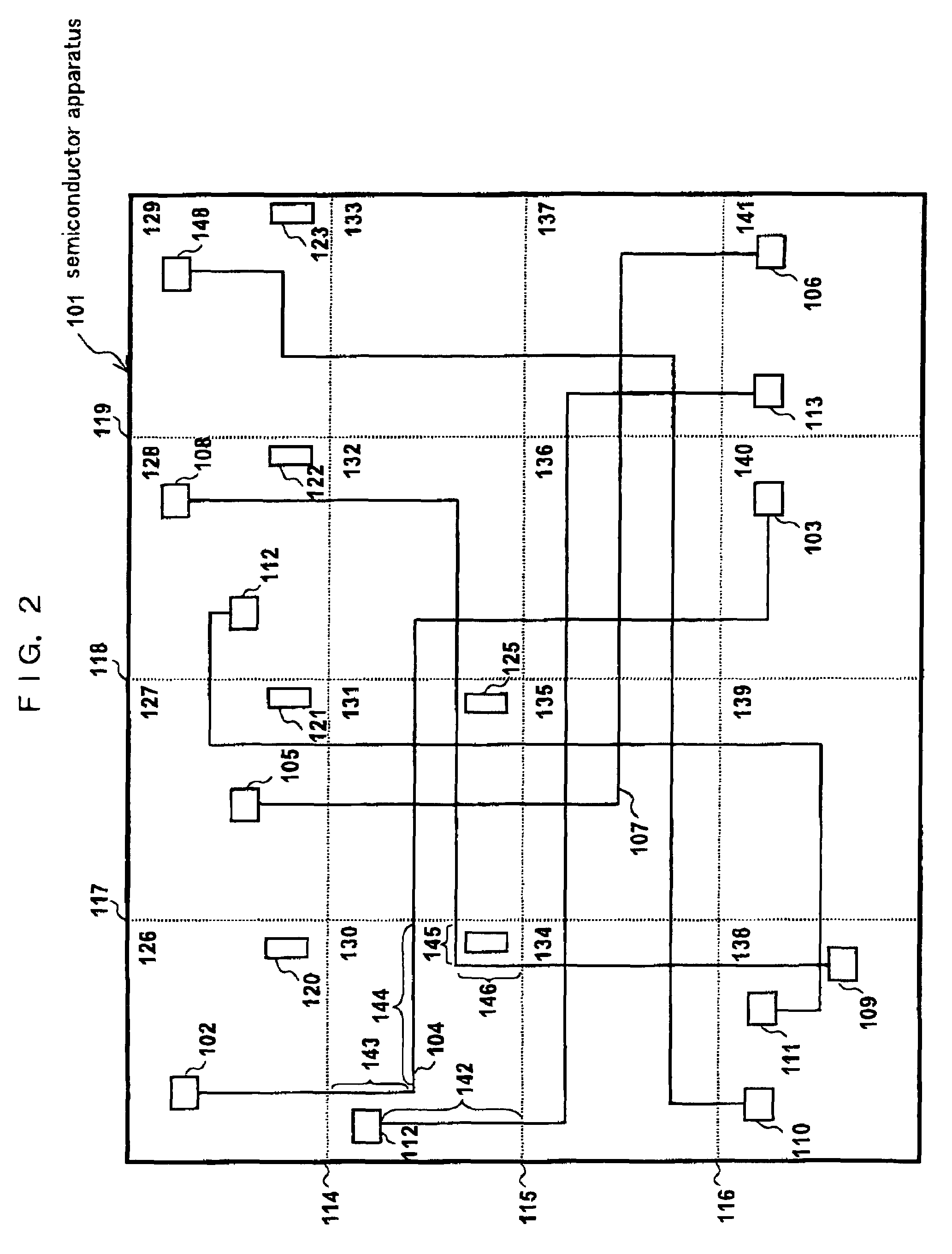
[0115]FIG. 2 shows a semiconductor apparatus according to an embodiment 3. A semiconductor apparatus 101 is divided by horizontal division lines 114, 115 and 116 and vertical division lines 117, 118 and 119 to thereby create divided regions 126-141. Each divided region includes a register, the register storing process information of the relevant divided region. The divided region 126 includes a register 120 storing the process information. The divided region 127 includes a register 121 storing the process information. The process-information registers are present in other divided regions as well.

[0116]Steps of the method of testing the semiconductor apparatus are as follows.[0117]1) The semiconductor apparatus 101 is divided into a plurality of divided regions as described.[0118]2) Registers present in the respective divided regions are extracted based on coordinates of the divided regions and registers.[0119]3) All of paths extending from the extracted registers to other registers ...


PUM

PropertyMeasurementUnit
delay timeaaaaaaaaaa
speedaaaaaaaaaa
time lengthaaaaaaaaaa

Abstract

A method of testing a semiconductor apparatus includes a step of dividing a region in the semiconductor apparatus into a plurality of divided regions, a step of extracting all of paths starting at registers and terminating at other registers present in the respective divided regions as candidate paths, a step of calculating delay times in signal transmissions of the candidate paths and selecting the candidate path having a maximum delay time in each divided region as a critical path, and a step of conducting a delay test for the critical path in each divided region to thereby accurately screen the semiconductor apparatus.

Description

BACKGROUND OF THE INVENTION[0001]The present invention relates to a method of testing a semiconductor apparatus.[0002]In the method of testing the semiconductor apparatus, a signal delay in a predetermined critical path is measured in order to guarantee a speed performance. The critical path is a path, of signal paths of logic circuits, configured in such manner that an erroneous operation is generated when a signal is not transmitted within a defined time length.[0003]As the semiconductor apparatus is more and more miniaturized, variation is generated in process parameters for each region in the same semiconductor apparatus. Further, delay time is accordingly variable. As a result, a path having an increased delay time in a signal transmission than an initially assumed critical path is generated, resulting in a failure to guarantee a predetermined operation speed.SUMMARY OF THE INVENTION[0004]Therefore, a main object of the present invention is to provide a method of testing a semi...

Claims


Application Information

Patent Timeline
Patent Type & Authority Patents(United States)
IPC IPC(8): G06F17/50G06K5/04G11B20/20G11B5/00G01R31/28G01R31/3185H01L21/822H01L27/04
CPCG06F17/5031G01R31/318583G06F30/3312
Inventor SHIMAMURA, AKIMITSU
Owner SOCIONEXT INC
Learn More