Method of production pitch fractionizations in semiconductor technology

a semiconductor technology and production method technology, applied in the field of production methods, can solve the problems of limited pitch value, limited method application, limited application, etc., and achieve the effect of reducing pitch by method steps

Active Publication Date: 2007-11-06
CHANGXIN MEMORY TECH INC
View PDF10 Cites 179 Cited by
  • Summary
  • Abstract
  • Description
  • Claims
  • Application Information

AI Technical Summary

Benefits of technology

[0005]In a further aspect, the invention decreases the pitch by method steps that are based on standard semiconductor technology.

Problems solved by technology

The value of the pitch is restricted by the production technology that is applied to structure the periodic pattern.
Some limitations are due to the mask technique that is employed in the structuring process.
These methods are only applicable if the structures that are produced are sufficiently precise to meet the requirements of the device performance.

Method used


Image

  • Method of production pitch fractionizations in semiconductor technology
  • Method of production pitch fractionizations in semiconductor technology
  • Method of production pitch fractionizations in semiconductor technology

Examples


Embodiment Construction

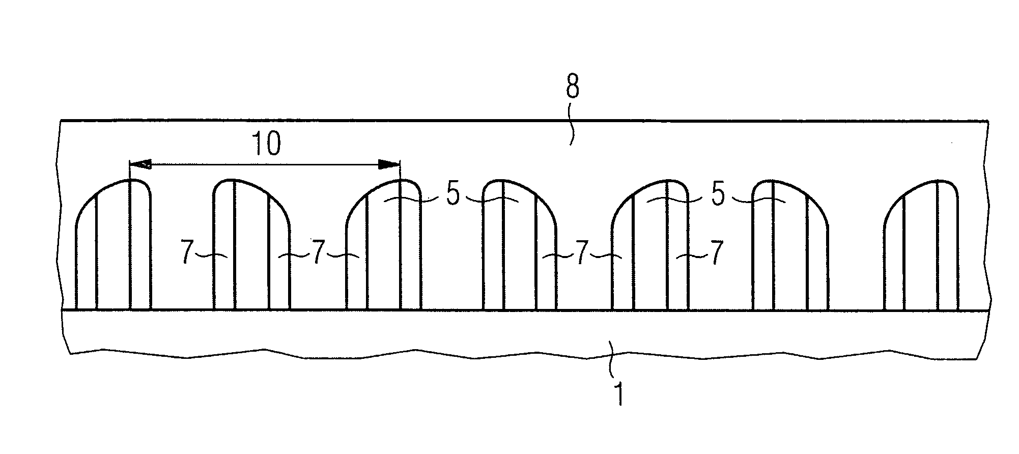
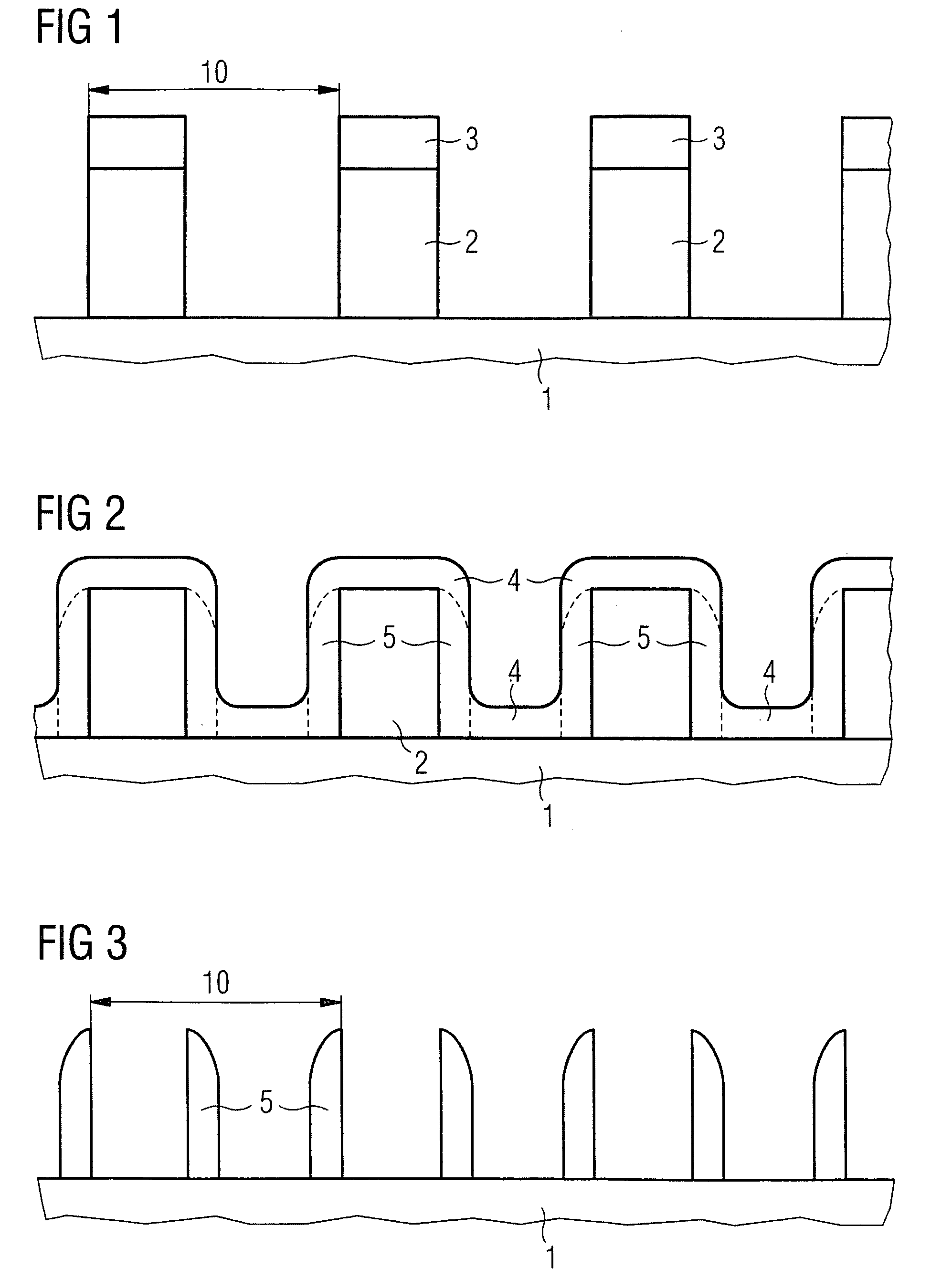
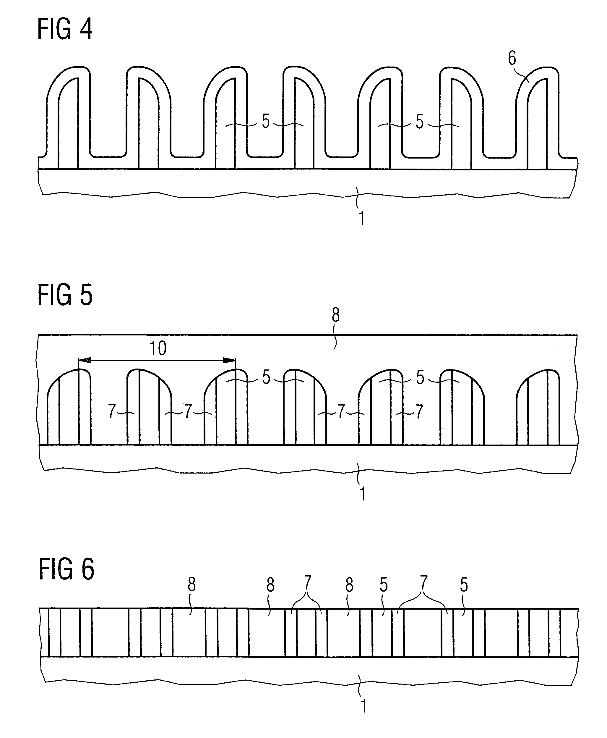
[0035]FIG. 1 shows a cross-section of a first intermediate product of a first variant of the method. A pattern layer 2 is applied on a main surface of a substrate 1, which may also comprise layers of different materials or semiconductor device structures. This is not shown in detail in FIG. 1, since it is not essential for the method to be described. The pattern layer 2 is provided with a structure of separate striplike parts running parallel to one another. This structure can be obtained by means of a hard mask 3. The hard mask 3 can be nitride, for example, which can be structured by a photolithography step including the application of a photo resist layer. The striplike parts of the pattern layer 2 have sidewalls, which are ideally perpendicular to the main surface of the substrate.

[0036]The lateral dimensions of the striplike parts, their widths, are the same throughout. The distances between two neighboring striplike parts are also the same for all pairs of neighboring parts. T...


PUM

PropertyMeasurementUnit
distanceaaaaaaaaaa
widthaaaaaaaaaa
thicknessaaaaaaaaaa

Abstract

Spacers are formed on sidewalls of striplike parts of a pattern layer of periodic structure. The pattern layer is removed, and the spacers are covered with a further spacer layer, which is then structured to second sidewall spacers. Gaps between the spacers are filled with a complementary layer. The upper surface is planarized to a lower surface level, leaving a periodic succession of the first spacers, the second spacers and the residual parts of the complementary layer. The lateral dimensions are adapted in such a manner that a removal of one or two of the remaining layers renders a periodic pattern of smaller pitch.

Description

TECHNICAL FIELD[0001]This invention concerns production methods of periodic structures or patterns of semiconductor devices.BACKGROUND[0002]Certain types of semiconductor devices like semiconductor memories comprise structure elements or patterned layers that are periodic at least in one dimension. Word lines and bit lines, for example, are often arranged along straight lines running parallel to one another. The width of the lines and the distance between neighboring lines are constant all over the device. Thus, the succession of the lines in one direction is periodic, preferably of minimal dimensions, which enables to realize a memory cell array of minimal area. The dimensions of the lines and their interspaces are continually repeated in the direction of the periodic succession. The length of one of these periods is called the pitch of the pattern.[0003]The value of the pitch is restricted by the production technology that is applied to structure the periodic pattern. Some limitat...

Claims


Application Information

Patent Timeline
Patent Type & Authority Patents(United States)
IPC IPC(8): H01L21/70
CPCH01L21/0337H01L21/32139H01L21/31144H01L21/0338
Inventor PARASCANDOLA, STEFANOCASPARY, DIRK
Owner CHANGXIN MEMORY TECH INC
Why Eureka
Try Eureka