Method for estimating the early failure rate of semiconductor devices

a technology of semiconductor devices and failure rates, applied in the field of semiconductor device testing, can solve the problem of requiring a small amount of samples for evaluation, and achieve the effect of facilitating accurate estimation of the early failure rate of an integrated circuit under customer use conditions

Active Publication Date: 2007-11-06
TEXAS INSTR INC
View PDF2 Cites 15 Cited by
  • Summary
  • Abstract
  • Description
  • Claims
  • Application Information

AI Technical Summary

Benefits of technology

[0004]Some embodiments of the invention provide numerous technical advantages. Other embodiments may realize some, none, or all of these advantages. For example, in one embodiment, more accurate estimation of the early failure rate of an integrated circuit under customer use conditions is facilitated. Several operating conditions may be accommodated (active and standby). Estimates may be scaled by die size to permit estimation of devices that have yet to be characterized. In some embodiments, an estimation method disclosed herein allows quick determination and optimization of minimum accelerated stress test conditions for a specified customer quality level. Furthermore, only a minimal amount of samples for evaluation may be required to estimate these minimum accelerated stress test conditions.

Problems solved by technology

Furthermore, only a minimal amount of samples for evaluation may be required to estimate these minimum accelerated stress test conditions.

Method used


Image

  • Method for estimating the early failure rate of semiconductor devices
  • Method for estimating the early failure rate of semiconductor devices
  • Method for estimating the early failure rate of semiconductor devices

Examples


Embodiment Construction

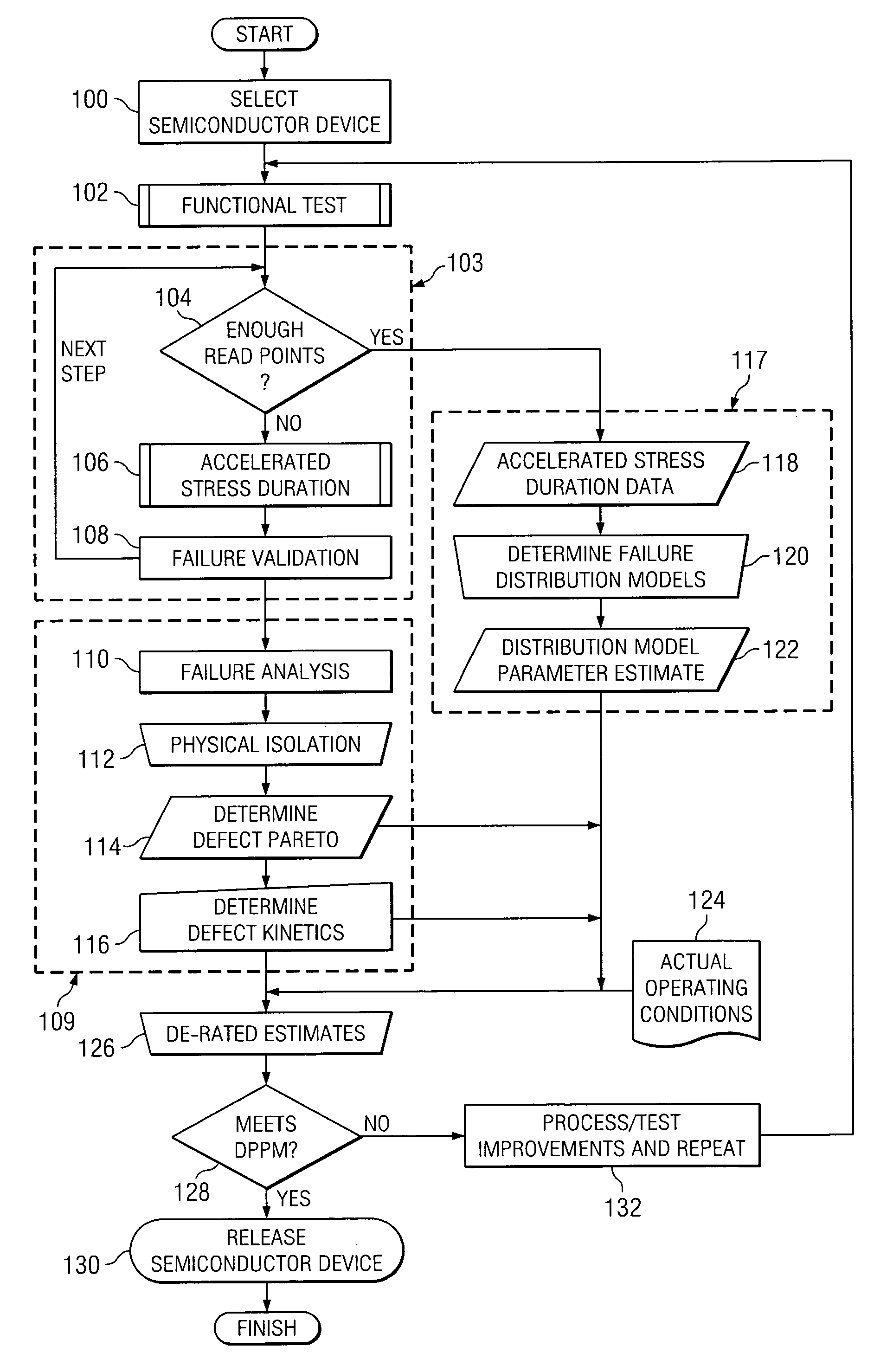
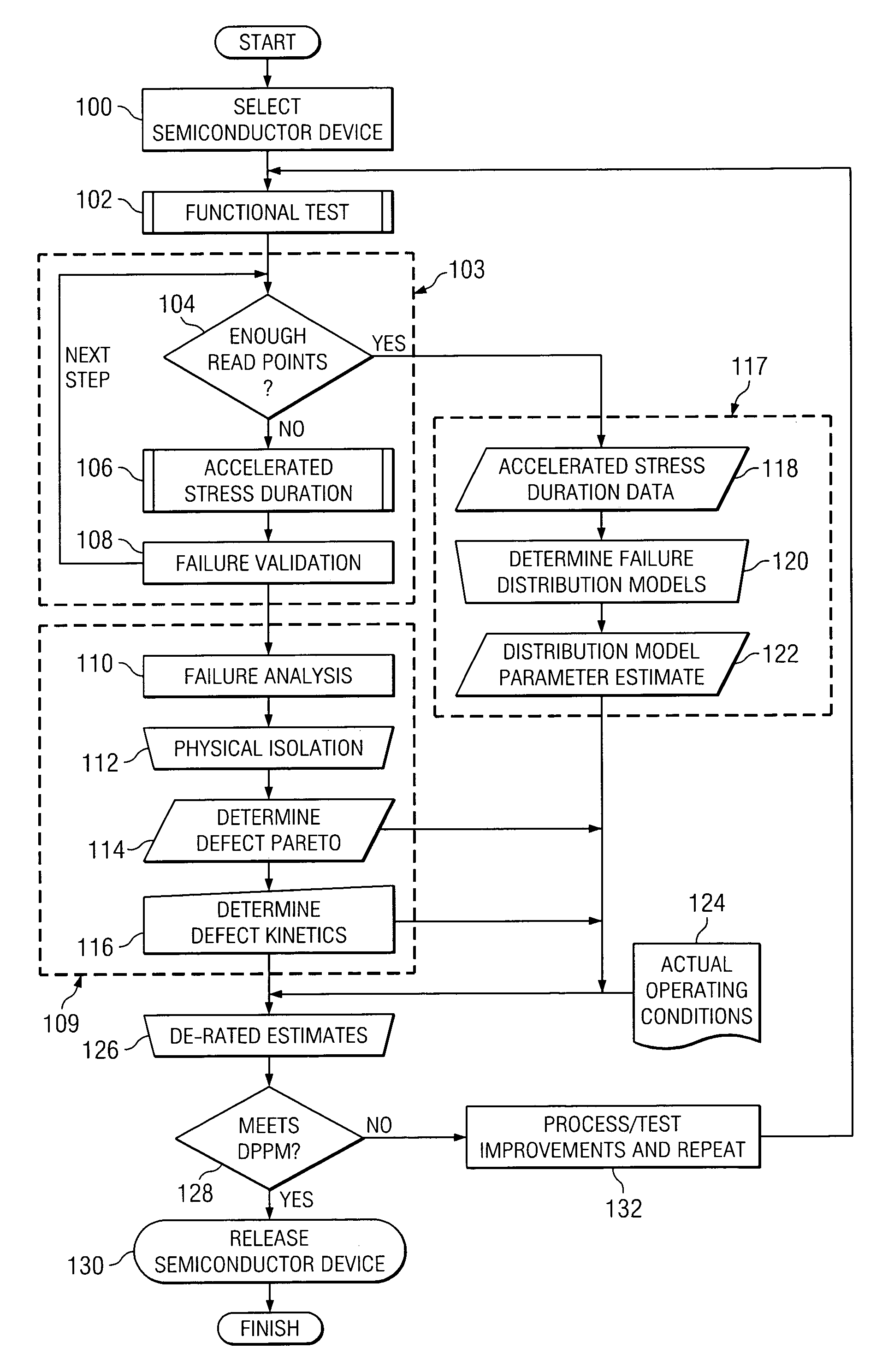
[0008]Example embodiments of the present invention and their advantages are best understood by referring now to FIG. 1 of the drawings, in which like numerals refer to like parts.

[0009]FIG. 1 is a flowchart illustrating an example method for estimating the early failure rate of semiconductor devices according to one embodiment of the present invention. The present invention contemplates the method outlined herein as being utilized with any suitable semiconductor devices, such as integrated circuits, within the teachings of the present invention. In addition, although the following detailed description discusses the defect ratio of semiconductor devices in defective parts per million (“DPPM”), the present invention contemplates the defect ratio of semiconductor devices being expressed in any suitable manner.

[0010]The example method begins at step 100 where a particular semiconductor device is selected. This semiconductor device may be a particular product, such as a particular integr...


PUM


Abstract

According to one embodiment of the invention, a method for estimating the failure rate of semiconductor devices includes obtaining accelerated stress duration data for a plurality of semiconductor devices, determining which of the semiconductor devices fail, classifying the defects for the failed semiconductor devices, determining a distribution model for the accelerated stress duration data, determining a set of parameters for the distribution model, determining a relative proportion of each defect classification to the total number of defect classifications, determining temperature and voltage acceleration factors for each defect classification, identifying actual operating conditions for the semiconductor devices, comparing the actual operating conditions for the semiconductor device with the distribution model, and determining a defect ratio for the semiconductor devices at the actual operating conditions for a predetermined time period based on the comparison.

Description

TECHNICAL FIELD OF THE INVENTION[0001]This invention relates generally to the field of semiconductor device testing and, more specifically, to a method for estimating the early failure rate of semiconductor devices.BACKGROUND OF THE INVENTION[0002]Understanding the defect levels of a semiconductor device during early use and the expected lifetime before wear out failure is important in many respects. This is the first experience a customer will have with the early reliability of a particular device. High temperature op-life (“HTOL”) may confirm product life capability. ATE Test and accelerated stress tests are classic methods employed to reduce early failure rates. For the extrinsic residual defects, one must be able to estimate the level defects, for example DPPM, which remain prior to product shipment to customers. Until the defect levels are acceptable, cycles of accelerated stress evaluation and defect screening or reduction are necessary. The synergy between effective test meth...

Claims


Application Information

Patent Timeline
Patent Type & Authority Patents(United States)
IPC IPC(8): G01R31/26
CPCG06F11/24G06F11/008
Inventor ANDERSON, THOMAS J.CARULLI, JR., JOHN M.
Owner TEXAS INSTR INC
Why Eureka
Try Eureka