Protection circuit for power management semiconductor devices and power converter having the protection circuit

a protection circuit and semiconductor technology, applied in the direction of electric devices, hybrid vehicles, pulse techniques, etc., can solve problems such as the peak voltage exceeding

Active Publication Date: 2007-11-13
HITACHI POWER SEMICON DEVICE
View PDF10 Cites 10 Cited by
  • Summary
  • Abstract
  • Description
  • Claims
  • Application Information

AI Technical Summary

Benefits of technology

[0021]It is possible to detect an occurrence of an overvoltage or an overcurrent caused ...

Problems solved by technology

As a result, if a thermal break occurs due to the overcurrent, or even if the overcurrent is cut off in high-speed, a peak voltage caus...

Method used


Image

  • Protection circuit for power management semiconductor devices and power converter having the protection circuit
  • Protection circuit for power management semiconductor devices and power converter having the protection circuit
  • Protection circuit for power management semiconductor devices and power converter having the protection circuit

Examples


first embodiment

A First Embodiment

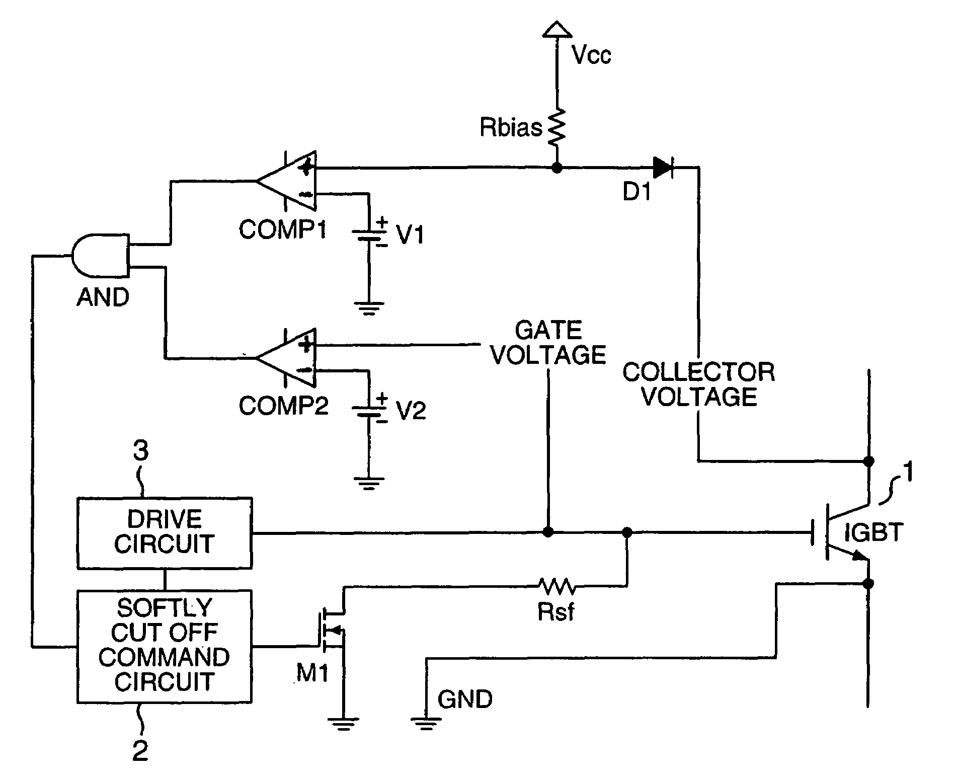
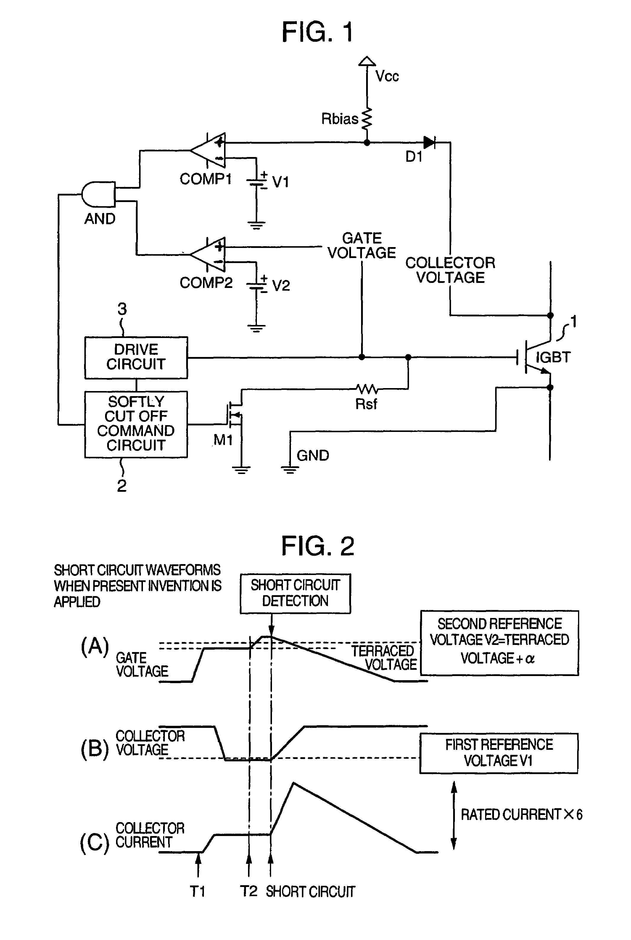
[0031]FIG. 1 is a circuit diagram generally illustrating a protection circuit for power management semiconductor devices of a first embodiment according to the present invention and illustrates an example in which an IGBT is used as a semiconductor device to be protected. FIG. 2 is a diagram generally illustrating waveforms for each voltage and current during switching of the power semiconductor device, the IGBT.

[0032]In FIG. 1, an output signal of a drive circuit 3 is supplied to a gate terminal of the IGBT 1, and the IGBT 1 is switched following an ON / OFF command signal of the drive circuit 3.

[0033]A collector terminal of the IGBT 1 is connected to a noninverting input port of a first comparator COMP 1 via a diode D1. An anode terminal of the diode D1 and the noninverting input port of the first comparator COMP 1 are connected to a line power voltage Vcc via a resistance Rbias. The resistance Rbias is a bias resistance for setting a conduction current value of th...

second embodiment

A Second Embodiment

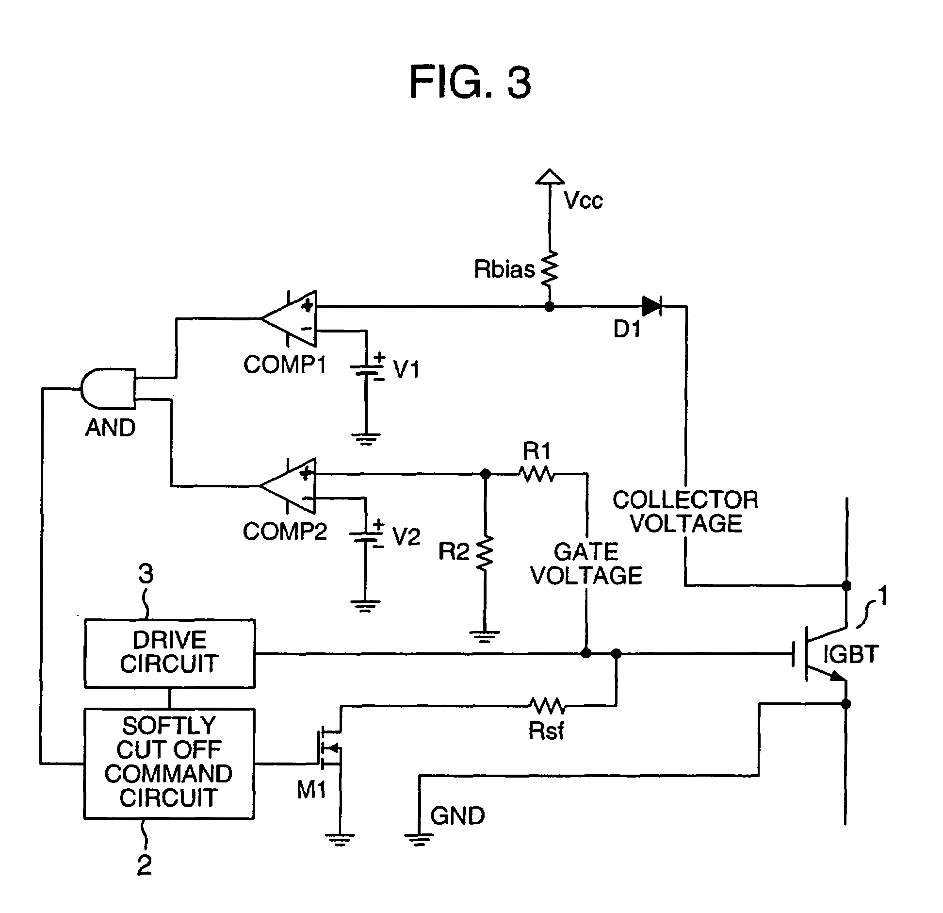
[0051]Next, a second embodiment of the present invention will be described with reference to FIG. 3. FIG. 3 is a diagram generally illustrating a protection circuit of power management semiconductor device as the second embodiment according to the present invention, and an example in which an IGBT is used as a semiconductor device to be protected.

[0052]In the second embodiment, resistances R1 and R2 are connected between a gate of the IGBT and a noninverting input port of a second comparator COMP 2. The second embodiment is structured identically to the first embodiment except that these resistances R1, R2 are connected. Therefore, detailed description of the second embodiment is omitted.

[0053]One end of the resistance R1 is connected to the gate of the IGBT 1, the other end of the R1 being connected to a noninverting input port of the second comparator COMP 2. One end of the resistance R2 is connected to the other end of the resistance R1 and the noninverting inp...

third embodiment

A Third Embodiment

[0057]FIG. 4 is a diagram generally illustrating a semiconductor integrated circuit mounted with a drive circuit including a protection circuit of a power management semiconductor device as a third embodiment according to the present invention.

[0058]A drive circuit comprising a pair of arms, upper and lower, for driving an IGBT is contained in one piece of semiconductor integrated circuit 15. The semiconductor integrated circuit 15 comprises line power terminals for each arm (VCT, VCC, GNT, GND), drive command input terminals (INT, INB), drive output terminals and protection detection operation terminals of the IGBT (SCT, SGT, PG, SFT, SCB, SGB, NG, SFB), and a protection detection output terminal (FL). Each of the upper and lower arms comprises a drive circuit and a short circuit protection circuit, and also comprises a level shift circuit for exchanging signals between the upper and lower arms.

[0059]The short circuit protection circuit of the semiconductor integr...


PUM


Abstract

A collector voltage of a power management semiconductor device is detected by a first comparator, and when the detected collector voltage exceeds a first reference voltage, the first comparator outputs a first detection signal. Furthermore, a gate voltage of the power management semiconductor device is detected by a second comparator, and when the detected gate voltage exceeds a second reference voltage, the second comparator outputs a second detection signal. The second reference voltage is a minimum gate voltage for feeding a rated power to the power management semiconductor device or over, and less than a line power voltage of a drive circuit of the power management semiconductor device. When both the first detection signal and second detection signal are being outputted, the gate voltage is reduced by a gate voltage reduction means so as to protect the power management semiconductor device from overcurrent and overvoltage.

Description

BACKGROUND OF THE INVENTION[0001]The present invention relates to a protection circuit for power management semiconductor devices for use in a semiconductor integrated circuit and a power converter having the protection circuit.[0002]As a power management semiconductor device for use in a power converter, a bipolar / MOS composite type semiconductor device (IGBT (Insulated Gate Bipolar Transistor)) has been widely used in recent years. The IGBT has a characteristic that while the amount of collector current to flow is determined by a gate voltage and a collector voltage, an increasing rate in the collector current associated with an increase in the collector voltage suddenly becomes larger as the gate voltage increases.[0003]When there occurs an arm short circuit or a load short circuit in the power converter, a line power voltage of the power converter is applied to the IGBT which is in ON operation and an excessive short circuit current flows due to above mentioned IGBT characterist...

Claims


Application Information

Patent Timeline
IPC IPC(8): H02H3/20H02H3/08H02H9/02H02H7/20B60L3/00H02H7/122H02M1/00H02M1/08H02M7/48H03K17/082H03K17/16
CPCB60K6/485B60L3/003B60W10/08H02M1/32H03K17/0828H03K17/168Y02T10/6226B60W20/00Y02T10/62H02H7/20
Inventor SASAKI, MASATAKAISHIKAWA, KATSUMISAITO, RYUICHISUDA, KOICHITAKAHASHI, KATSUAKI
Owner HITACHI POWER SEMICON DEVICE
Why Eureka
Try Eureka