Method and imaging apparatus for correcting defective pixel of solid-state image sensor, and method for creating pixel information

a solid-state image sensor and pixel information technology, applied in the direction of radiation control devices, color signal processing circuits, packaging foodstuffs, etc., can solve the problem of defective pixel not being able to capture a pixel value on a local basis, image captured through correct exposure may seem somewhat unsatisfactory compared to a silver halide photograph, and significant image quality degradation

Inactive Publication Date: 2007-11-27
FUJIFILM CORP
View PDF17 Cites 10 Cited by
  • Summary
  • Abstract
  • Description
  • Claims
  • Application Information

AI Technical Summary

Benefits of technology

[0031]According to the present invention, pixel information for defining as a defective pixel a pixe

Problems solved by technology

A solid-state image sensor such as a charge-coupled device (CCD), used in a digital camera or the like has a very small dynamic range compared to a general silver halide photograph, and therefore even an image captured through correct exposure may seem somewhat unsatisfactory compared to a silver halide photograph.
Moreover, so called loss of shadow detail and burnt highlight may occur, resulting in significant degradation in image quality depending on image-capturing conditions.
The solid-state image sensor of a CCD or the like is produced by forming a large number of photosensitive elements such as photodiodes on a semiconductor substrate but in production of the image sensor, a defective pixel unable to capture a pixel value on a local basis may occur due to impurities introduced in th

Method used


Image

  • Method and imaging apparatus for correcting defective pixel of solid-state image sensor, and method for creating pixel information
  • Method and imaging apparatus for correcting defective pixel of solid-state image sensor, and method for creating pixel information
  • Method and imaging apparatus for correcting defective pixel of solid-state image sensor, and method for creating pixel information

Examples


Embodiment Construction

[0053]The preferred embodiment of the present invention will be described in detail according to the attached drawings.

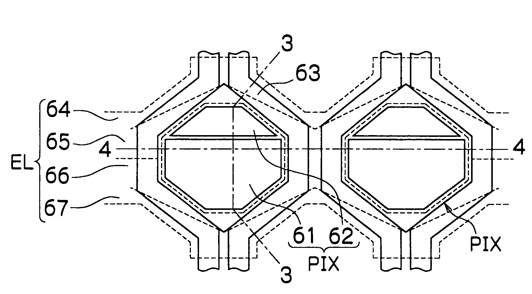
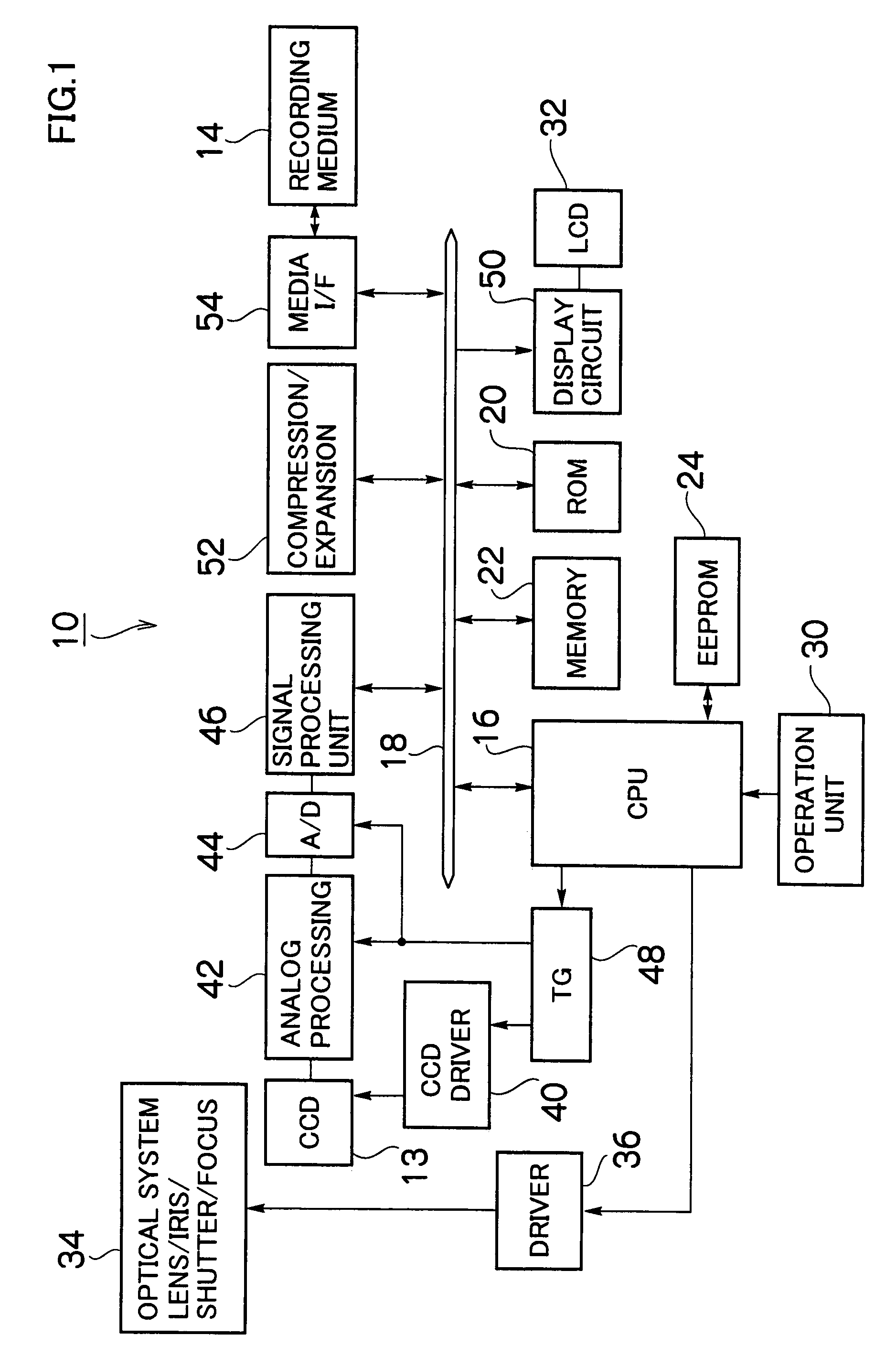
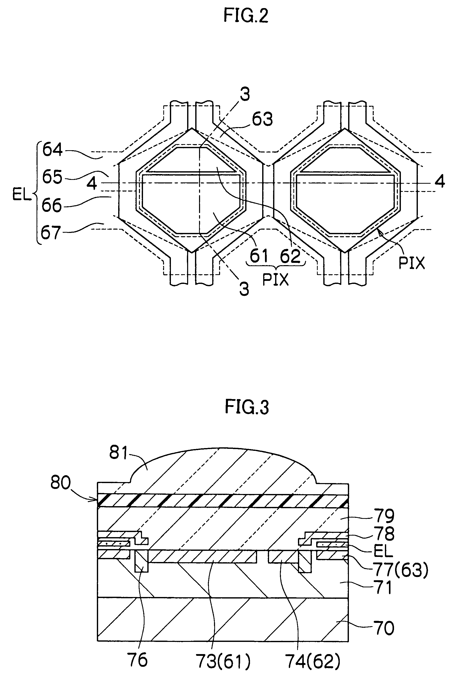
[0054]FIG. 1 is a block diagram showing the configuration of an electronic camera according to an embodiment of the present invention. The camera 10 is a digital camera converting into digital image data an optical image of a subject captured through a CCD solid-state image sensor (hereinafter referred to as CCD) 13, and a method for correcting a defective image according to an embodiment of the present invention is applied to part of a signal processing device which processes an image signal obtained from the CCD 13.

[0055]The overall operation of the camera 10 is generally controlled by a central processing unit (CPU) 16 built in the camera 10. The CPU 16 functions as a control device which controls a main camera system according to predetermined programs, and functions as a computation device which performs a various kinds of computations such as automatic exposur...


PUM


Abstract

In a solid-state image sensor in which a large number of pixel cells each comprised of a combination of a main photosensitive pixel having a relatively large area and a subsidiary photosensitive pixel having a relatively small area are arranged, if the subsidiary photosensitive pixel has a defect for any pixel cell, division photometry data during AE processing is read, and the defective pixel is replaced with a value obtained by dividing the output value of the main photosensitive pixel at the same position by a sensitivity ratio only for a section for which it is determined that the main photosensitive pixel is not saturated. Thus, the pixel value of a defective pixel can be accurately corrected without causing a reduction in resolution sensitivity compared to a conventional method of correcting a defective pixel using surrounding pixel information.

Description

[0001]This Nonprovisional application claims priority under 35 U.S.C. § 119(a) on Patent Application No(s). 2003-009943 and 2003-091948 filed in JAPAN on Jan. 17, 2003 and Mar. 28, 2003, the entire contents of which are hereby incorporated by reference.BACKGROUND OF THE INVENTION[0002]1. Field of the Invention[0003]The present invention relates to a method and an imaging apparatus for correcting a defective pixel of a solid-state image sensor, and particularly to a technique that is applied to an electronic image recording apparatus such as a digital camera or movie camera, which is a signal processing technique for correcting defects (flaws) in photosensitive pixels that may occur in production of a solid-state image sensor. The present invention further relates to a digital camera which comprises an imaging device having two types of light-receiving elements of different light-receiving sensitivities and light-receiving signal saturation levels for each pixel, and a method for cre...

Claims


Application Information

Patent Timeline
IPC IPC(8): H04N9/64H01L27/148H01L31/10H04N5/225H04N5/335
CPCH04N5/367H04N25/68A61J1/03A61J7/04
Inventor KOBAYASHI, HIROKAZUODA, KAZUYAMISAWA, TAKESHI
Owner FUJIFILM CORP
Why Eureka
Try Eureka