Semiconductor memory device

a memory device and semiconductor technology, applied in the field of semiconductor memory devices, can solve the problems of reducing the number of output buffer circuits operating simultaneously, reducing the noise generated by the operation of the output buffer circuit, and so as to reduce the noise only without sacrificing the readout ra

Active Publication Date: 2007-11-27
TAMIRAS PER PTE LTD LLC
View PDF5 Cites 7 Cited by
  • Summary
  • Abstract
  • Description
  • Claims
  • Application Information

AI Technical Summary

Benefits of technology

[0032]The present invention has been made in view of the aforementioned problems. An object of the present invention is to provide a semiconductor memory device capable of reducing noise generated in consequence of the simultaneous switching of plural output buffers 63, and stably operating at high speed.
[0038]According to the semiconductor memory device of the present invention, by providing plural control signal lines for controlling the timings for operating the output buffer circuits, the operation timings of the output buffer circuits can be displaced, and the number of the output buffer circuits operating simultaneously can be reduced, with the result that noise generated by the operations of the output buffer circuits can be reduced.
[0039]In addition, by controlling the output buffer circuit operating finally so as to operate at the exactly same timing as that of the conventional semiconductor memory device, it is possible to reduce only noise without sacrificing a readout rate.

Problems solved by technology

There is a problem that, in the event of the simultaneous switching of many of these output buffers 63, large noise generates due to the instantaneous flowing of large through current to induce erroneous operations to the peripheral apparatuses and own circuits.
Besides, when the noise reduction method disclosed in the aforementioned publications is applied to a semiconductor memory device, in consequence of the displacement of the output timings, readout rate is delayed by the displaced time.
As such, in the case of using any of the aforementioned methods for a semiconductor memory device, there arises a problem of exerting an adverse effect to the readout rate.

Method used


Image

  • Semiconductor memory device
  • Semiconductor memory device
  • Semiconductor memory device

Examples


Embodiment Construction

[0047]Hereinafter, description will be given of an embodiment of the present invention with reference to the drawings.

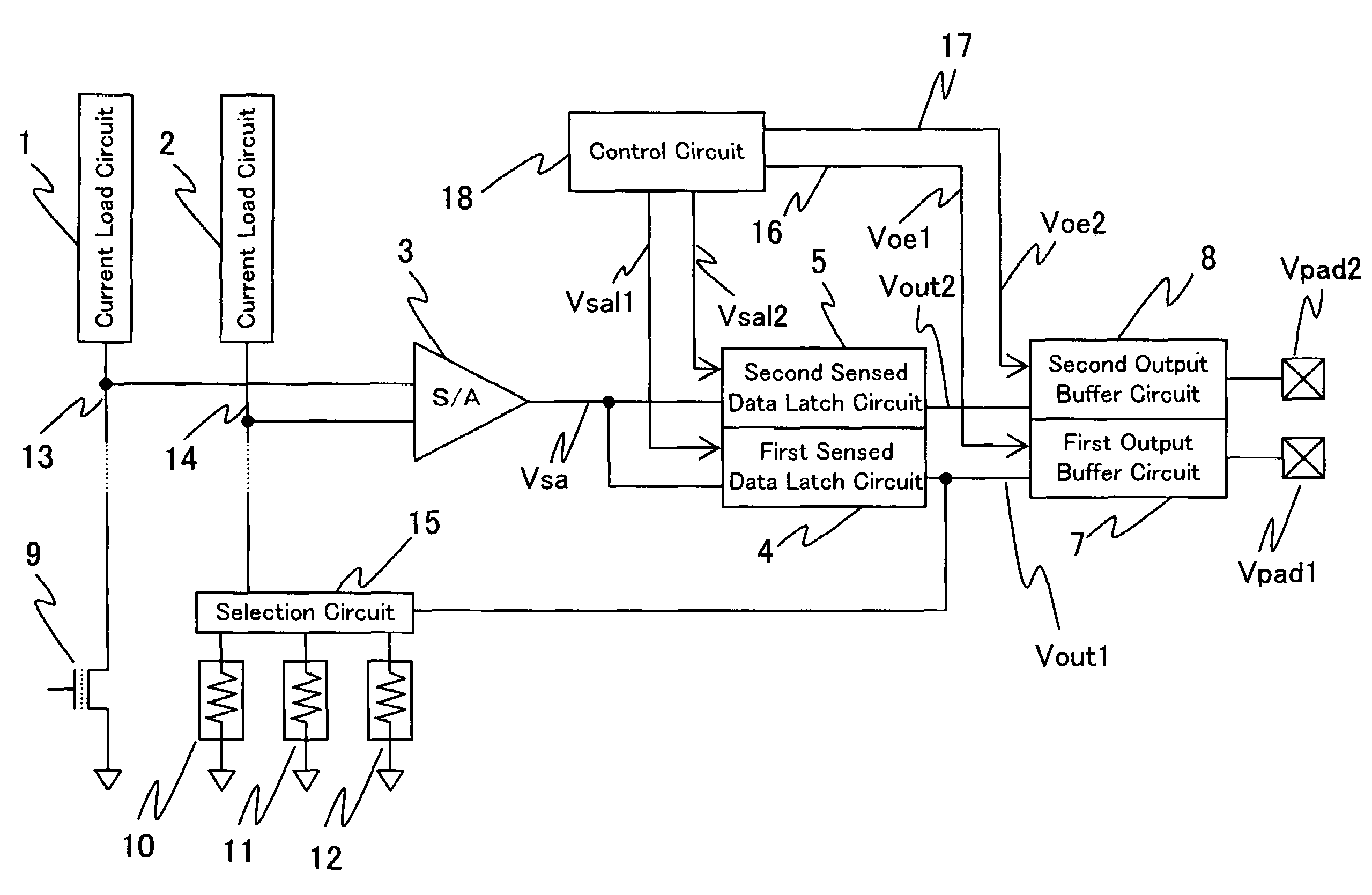
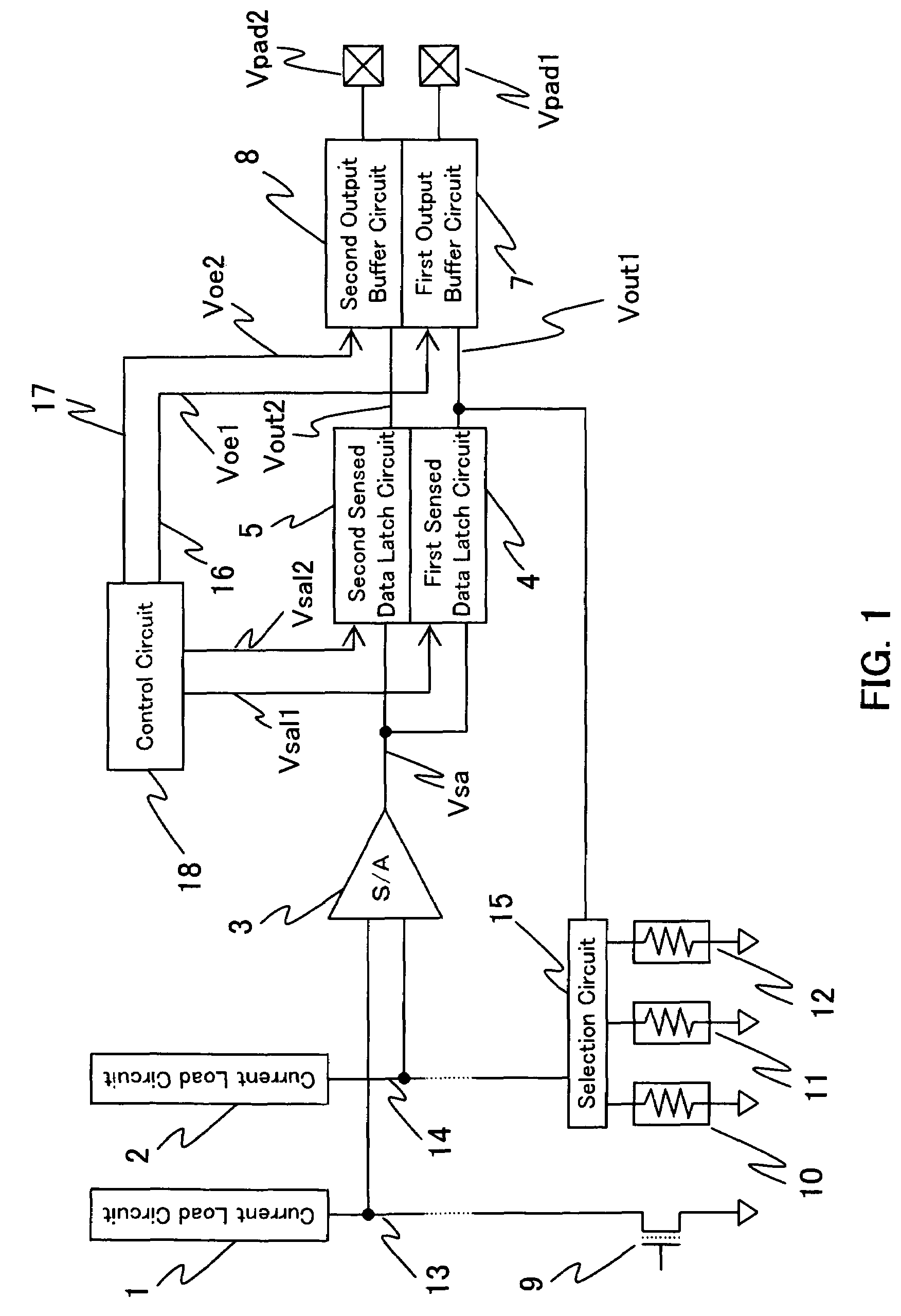
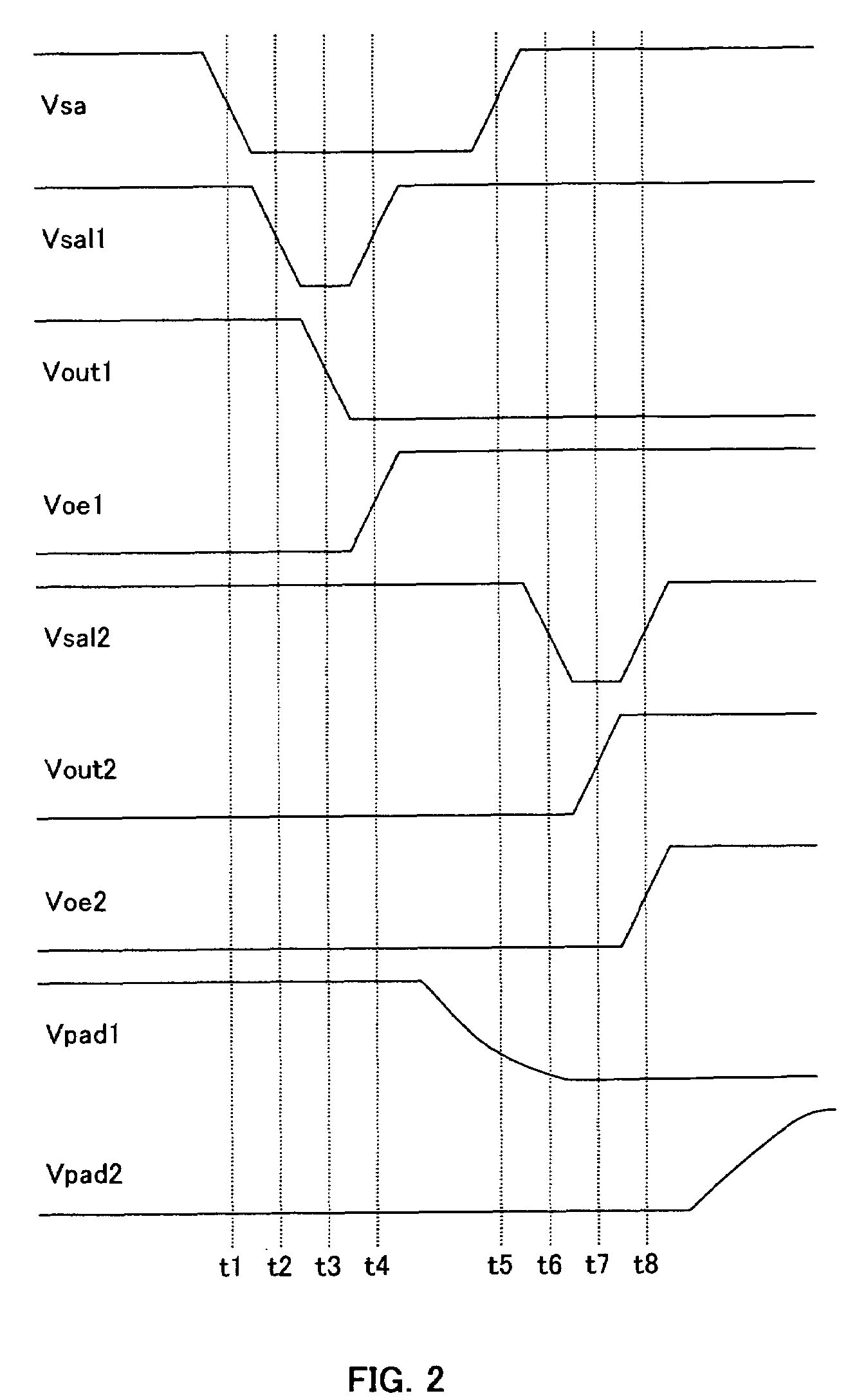
[0048]FIG. 1 is a block diagram showing an embodiment of a semiconductor memory device according to the present invention (hereinafter, appropriately referred to as “inventive device”). Herein, components having the same constitutions as those of the conventional components are denoted by the same reference numerals. The constitutional difference between this embodiment shown in FIG. 1 and the conventional embodiment shown in FIG. 3 is as follows. That is, the inventive device has a control signal line 16 for controlling the operation timing of a first output buffer circuit 7 by a first sensed data output control signal Voe1 from a control circuit 18 and a control signal line 17 for controlling the operation timing of a second output buffer circuit 8 by a second sensed data output control signal Voe2 from a control circuit 18. With the control signal lines 16, 17 fro...


PUM


Abstract

In a semiconductor memory device for reading out multilevel data in a time-shared manner at different timings, by providing plural control signal lines for controlling the operation timings of the output buffer circuits, the operation timings of output buffer circuits can be displaced, and the number of output buffer circuits operating simultaneously can be decreased, with the result that noise is reduced. Besides, by allowing the output buffer circuit, which outputs data read out early in a time-shared manner, to operate at an early timing, data output is terminated without retarding the operation timing of the output buffer circuit operating at the last timing.

Description

CROSS REFERENCE TO RELATED APPLICATION[0001]This Nonprovisional application claims priority under 35 U.S.C. §119(a) on Patent Application No. 2005-075611 filed in Japan on Mar. 16, 2005, the entire contents of which are hereby incorporated by reference.BACKGROUND OF THE INVENTION[0002]1. Field of the Invention[0003]The present invention relates to a semiconductor memory device, in particular, a semiconductor memory device having a data readout scheme based on a time-shared sensing scheme for reading out data of plural bits stored in a single memory cell in a time-shared manner.[0004]2. Description of the Related Art[0005]In general, a readout circuit of a semiconductor memory device supplies a current to a memory cell storing information, compares the current flowing through the memory cell (cell current) with a reference current, and determines whether the cell current is larger or smaller than the reference current, thereby taking out the information written in the memory cell. As...

Claims


Application Information

Patent Timeline
Patent Type & Authority Patents(United States)
IPC IPC(8): G11C7/00
CPCG11C7/1012G11C7/1051G11C7/106G11C11/5642G11C16/28G11C7/1066G11C16/32H04M1/0264H04N23/55
Inventor ANZAI, SHINSUKEWATANABE, MASAHIKOYOSHIMOTO, TAKAHIKO
Owner TAMIRAS PER PTE LTD LLC
Why Eureka
Try Eureka