Tuneable unipolar lasers

a laser and unipolar technology, applied in the field of unipolar lasers, can solve the problems of limited wavelength tunability, inherently limited emission wavelength, and conventional semiconductor lasers based on band-band transitions within p-n- junctions, and achieve the effect of increasing the back facet reflectivity, reducing the threshold current of any given laser length l, and increasing the reflectivity

Active Publication Date: 2007-11-27
NANOPLUS GMBH
View PDF29 Cites 5 Cited by
  • Summary
  • Abstract
  • Description
  • Claims
  • Application Information

AI Technical Summary

Benefits of technology

[0017]If a metal is used to form the lattice structure, the advantageous effects described in the foregoing can be achieved to a particularly comprehensive extent. Irrespective of the material selected to construct the lattice structure, the lattice structure can also be formed by material removal, not only by material application. In particular, the lattice structure can be formed as an overlying structure (e.g., a metal lattice structure), as well as defined into the upper cladding layer by an etched structure and successive filling of the resulting grooves by other material (e.g., a metal). Important in this context is the close contact between lattice structure and upper metallic electrode for efficient current injection to each of the cavity segments. If a metal is used to define the lattice structure, it is particularly advantageous to use the same metal also for the fabrication of the top contact layer to each section. In particular, a metal layer sequence (e.g., Cr, Pt, Au layers of various thickness) can also be used for this purpose. In order to improve the electrical injection, it proves advantageous for the sides of the waveguide ridge to be arranged substantially at right angles to the plane in which the lattice structure extends.
[0018]The typical semiconductor unipolar laser includes opposed front and back surfaces, referred to as front and back facets. These facets are typically obtained by cleaving. In order to control the light output and to direct it as desired, for example preferentially to the front side, it might become necessary to increase the back facet reflectivity. Furthermore in order to realize other properties of the device, e.g., small threshold currents, it may be advisable to also increase the reflectivity at the front surface. The threshold current for laser onset is proportional to exp[2(αi+αm) / Γgo], where Γis the confinement factor, go is the material gain, αi is the internal absorption and αm=1 / L*ln(1 / R) are the mirror losses. Therefore the threshold current for any given laser length L can be significantly reduced if the resonator reflectivity R is increased. By increasing the reflectivity, i.e., decreasing the mirror losses αm, the length L of the device can be simultaneously reduced without a significant loss of performance as compared to lasers of the same lengths without additional reflectors. By using high facet reflectivities, the slope efficiency, i.e., the output power dependence on the drive current, can also be increased as compared to lasers with cleaved facets using highly reflective mirrors on one or both ends of the ridge.
[0019]This increase in reflectivity might, for example, be obtained by defining a Bragg reflector structure adjacent to the laser facet(s). Typically a Bragg reflector structure is realized by applying different dielectric materials of appropriate thickness to the facets. Since many dielectric materials have absorbing properties in the wavelength range of interest, a particularly useful approach for a unipolar laser is the definition of a Bragg reflector using an air-semiconductor mirror structure. These reflectors are arranged perpendicular to the laser ridge at a certain distance from one or both ends. The width of the mirror plates as well as the width of the air gap depend on the emission wavelength of the device. The dimensions of the mirror plates can extend beyond the ridge width dimensions to reduce diffraction losses of the laser light. By such a unipolar laser with Bragg mirrors at one or both end facets, particularly low current densities and high output powers can be achieved. This can be used to increase the upper temperature of laser operation with respect to devices with cleaved facets. The Bragg mirrors can be realized as mirror plates separated by gaps. Alternatively they can also be realised by a two dimensional periodic pattern involving for example air holes. In both cases the change of refractive index can be used to modify the reflectivity compared to cleaved facets. Similar structures can also be used to control the coupling between the unipolar laser segments. However, the Bragg mirrors are optional structures to modify the facet ref lectivities which can be omitted if desired.
[0020]In a process according to some embodiments of the invention, on a base consisting of a semiconductor substrate, a complete unipolar semiconductor laser structure is produced in an epitaxial process with the subsequent formation of a waveguide ridge. This waveguide ridge is divided into a plurality of cavity sections by subjecting the semiconductor laser structure to a material removal process and the subsequent application of a lattice structure to various cavity sections. Irrespective of the material selected to form the lattice structure, the lattice structure can also be produced by material removal, not only by material application.
[0021]A processes according to some embodiments of the invention as briefly described in the foregoing thus facilitates the production of functional lasers in a first process phase, thereby facilitating the precise checking and determination of the electrical and optical properties, for example determination of the individual amplification spectrum of the epitaxial unipolar laser structure used for the laser fabrication. Only thereafter in a second process phase, by the formation of cavity segments and lattice structures with defined parameters, are single-mode tuneable unipolar lasers obtained.
[0022]In those embodiments in which the lattice structure is produced by the application of a lattice, the use of a lithographic process, for example by optical or electron beam lithography with subsequent etching of the lattice followed by a metallization, proves particularly advantageous.

Problems solved by technology

Conventional semiconductor lasers are based on band-band transitions within a p-n- junction and are inherently limited in the maximal attainable emission wavelength.
Thus, conventional DFB unipolar lasers exhibit a narrow linewidth as advantageous for sensing and other applications, but the wavelength tunability is limited.

Method used


Image

  • Tuneable unipolar lasers
  • Tuneable unipolar lasers
  • Tuneable unipolar lasers

Examples


Embodiment Construction

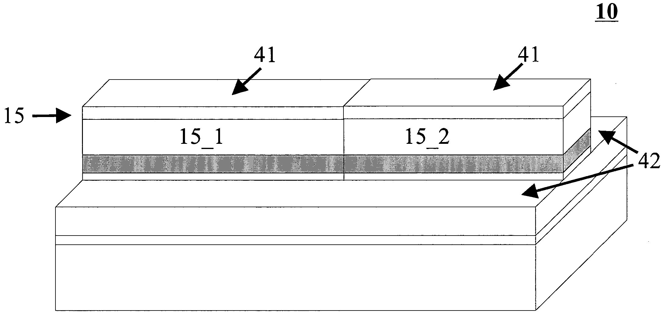
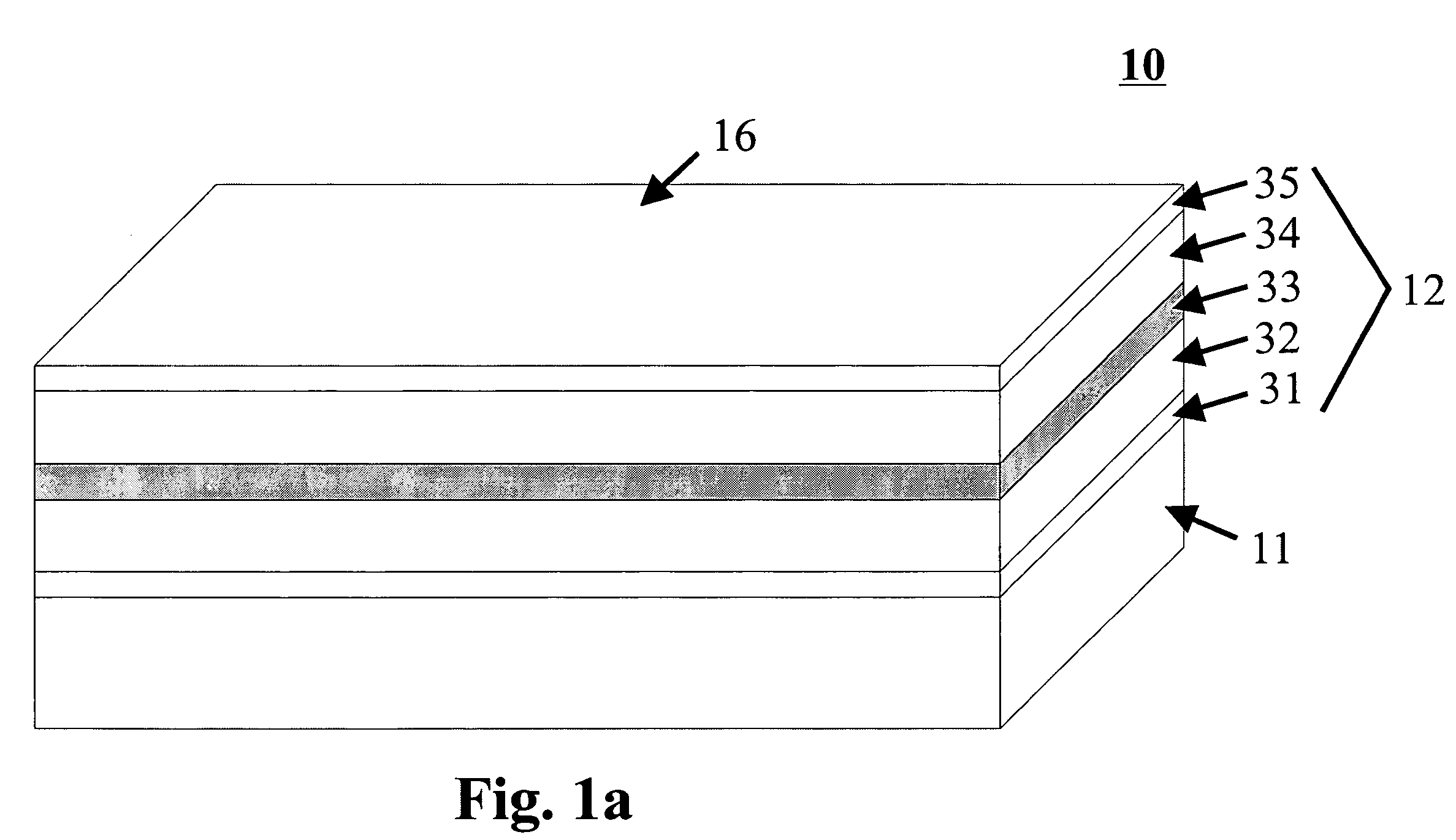
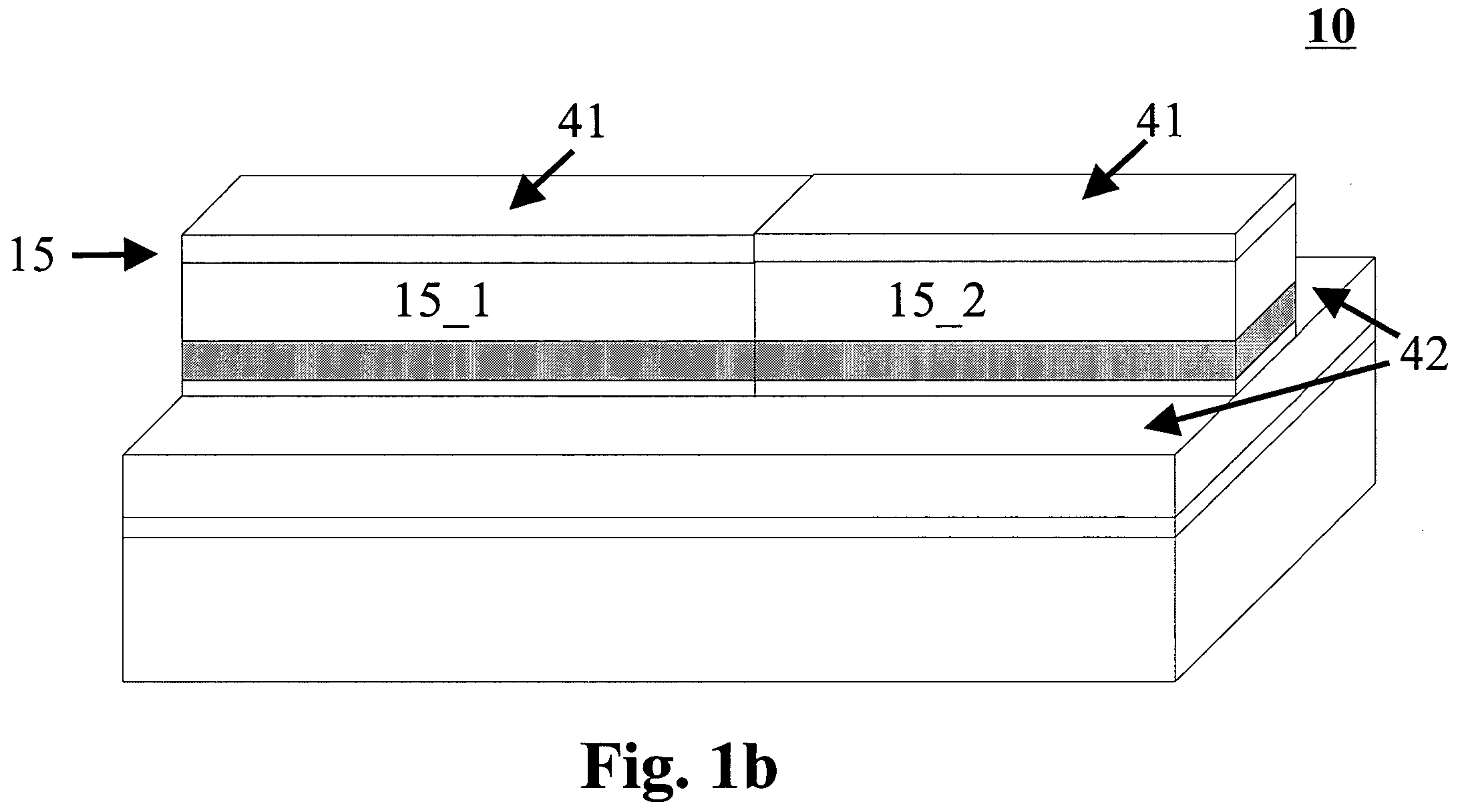
[0039]FIGS. 1a-1d illustrate typical steps in the fabrication of a tunable unipolar laser 10. Referring to the drawings in particular, FIG. 1a is a simplified perspective view of an exemplary tunable unipolar laser 10 comprising a semiconducting substrate 11 and an epitaxial structure 12 grown thereon. The epitaxial structure comprises a lower cladding layer 31, a lower guiding layer 32, an active region 33 suitable for lasing in a region of wavelengths around a wavelength λ, an upper guiding layer 34 and an upper cladding layer 35 having an upper surface 16. Semiconducting substrate 11 and epitaxial structure 12 contain doped semiconductor material of only one conductivity type (either only n-type or only p-type). For a wide tuning range of the laser, an active region with an engineered broad spectral gain region is advantageous.

[0040]In an exemplary embodiment of the invention, the active region is designed for laser emission at an infrared wavelength λ around 9.5 μm. The active r...


PUM


Abstract

A unipolar semiconductor laser is provided in which an active region is sandwiched in a guiding structure between an upper and lower cladding layer, the lower cladding layer being situated on a semiconducting substrate. The unipolar semiconductor laser comprises a raised ridge section running from end to end between end mirrors defining the laser cavity. The ridge section aids in optical and electrical confinement. The ridge waveguide is divided in a plurality of cavity segments (at least two). Lattice structures can be arranged on and / or adjacent to these cavity segments. Each cavity segment is in contact with upper metallic electrodes. A metallic electrode coupled to the bottom surface of the semiconducting substrate facilitates current injection through the device.

Description

FIELD OF THE INVENTION[0001]The present invention relates to unipolar lasers with a semiconductor substrate, a laser structure containing an active region sandwiched in a waveguide structure and arranged on the semiconductor substrate, a waveguide ridge divided into a plurality of cavity segments (at least two) and separate contacts to each of the cavity segments. Each of the cavity segments of the waveguide ridge can carry a specially designed lattice structure at a distance from the active region. The present invention further relates to a technological process for the production of such a widely tunable unipolar laser.BACKGROUND OF THE INVENTION[0002]Conventional semiconductor lasers are based on band-band transitions within a p-n- junction and are inherently limited in the maximal attainable emission wavelength. In contrast, for unipolar laser devices, i.e., lasers based on the injection of one type of carrier, no comparable long wavelength limit exists. The operating principle ...

Claims


Application Information

Patent Timeline
Patent Type & Authority Patents(United States)
IPC IPC(8): H01S5/00H01S3/082H01S5/12H01S5/34
CPCB82Y20/00H01S5/3402H01S5/12H01S5/1021H01S5/1215
Inventor FISCHER, MARC OLIVERFORCHEL, ALFRED
Owner NANOPLUS GMBH
Why Eureka
Try Eureka