Integrated circuit having independently formed array and peripheral isolation dielectrics

a technology of isolation dielectrics and integrated circuits, which is applied in the field of integrated circuits with independently formed arrays and peripheral isolation dielectrics, can solve the problems of intolerant to low levels, inability to infuse unique characteristics into separate isolation dielectrics, and inability to meet diverging specifications of memory cells and peripheral transistors contemporaneously formed isolation dielectrics, etc., to achieve the effect of eliminating overlap, facilitating the creation of floating gates, and reducing cell siz

Inactive Publication Date: 2007-12-04
TEXAS INSTR INC
View PDF13 Cites 0 Cited by
  • Summary
  • Abstract
  • Description
  • Claims
  • Application Information

AI Technical Summary

Benefits of technology

[0009]In accordance with the teachings of the present invention, an integrated circuit having independently formed array and peripheral isolation dielectrics is provided that substantially eliminates or reduces the disadvantages associated with the prior techniques and processes.
[0011]The invention has several important technical advantages. The dielectric isolation regions of the array are formed independently of the peripheral dielectric regions. Peripheral dielectric regions may be formed to a desired thickness for high voltage devices, while array dielectric regions may be scaled to minimize cell size. Additionally, the invention eliminates overlap between the distal ends of the floating gates and the isolation dielectric residing between the gates. The area of substrate supporting each floating gate may be maintained or increased despite the scaling of the floating gate width. A good read current is, therefore, maintained without creating stress-induced leakage current by thinning the gate oxide layer. Eliminating overlap between the floating gates and the isolation dielectric also facilitates creation of floating gates with little or no topography, making it easier to remove all polysilicon from between the floating gates. Use of relatively flat polysilicon layers solves problems associated with floating gate shorts caused by residual polysilicon residing between the floating gates. Also, because the floating gates do not extend beyond the trench corners, problems associated with oxide thinning such as nonuniformities in data retention and threshold voltages are reduced or eliminated.

Problems solved by technology

One problem with this approach is that it is difficult to instill unique characteristics into the separate isolation dielectrics because they are formed contemporaneously.
An approach that contemporaneously forms isolation dielectrics for memory cells and peripheral transistors cannot satisfy theses diverging specifications.
Another problem with this approach is that as the memory cells are scaled, they become intolerant to low levels of leakage current.
Decreasing this area width without reducing the gate oxide thickness results in degradation of the cell's read current.
Unfortunately, it is often impractical to decrease the gate oxide thickness because this leads to high levels of stress-induced leakage current.
Therefore, it is difficult to scale these devices without either degrading the cell's read current or making them susceptible to stress-induced leakage currents.
Another problem with this approach is that the overlapping regions result in complex device topography, making it difficult to etch all of the polysilicon from the areas between floating gates.
Failure to remove all of the polysilicon between floating gates may cause adjacent floating gates to short out.
Still another problem with this approach is that when used in conjunction with a configuration comprising trenches and moats within the substrate, the gate oxide layer tends to thin around the trench corners, causing data retention and threshold voltage nonuniformities.

Method used


Image

  • Integrated circuit having independently formed array and peripheral isolation dielectrics
  • Integrated circuit having independently formed array and peripheral isolation dielectrics
  • Integrated circuit having independently formed array and peripheral isolation dielectrics

Examples


Embodiment Construction

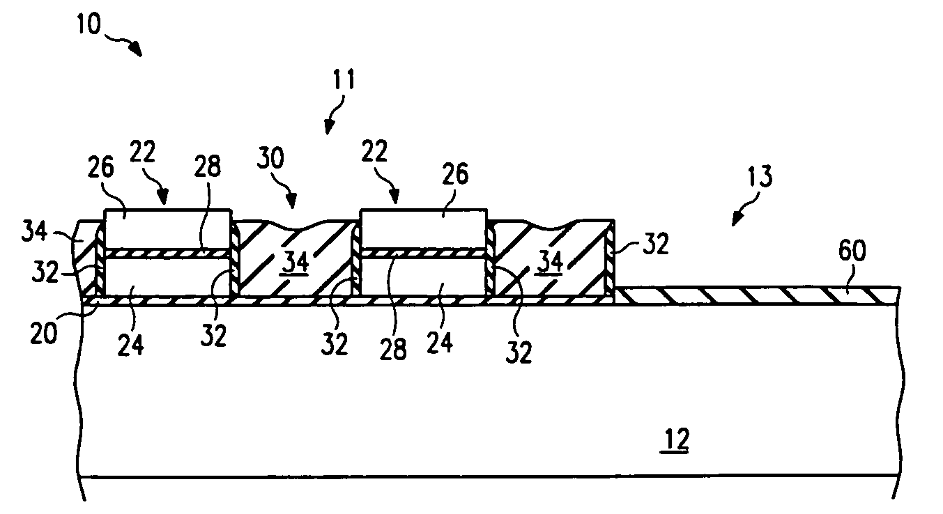
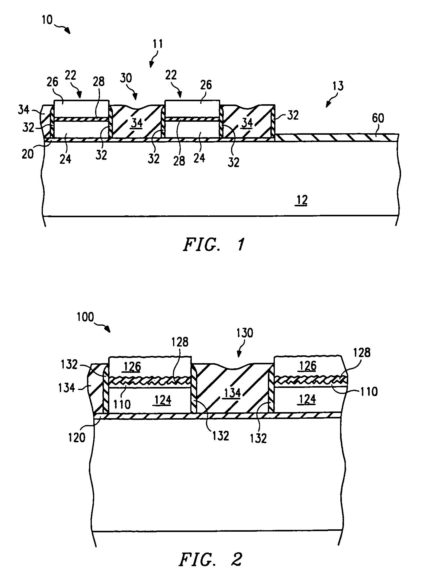
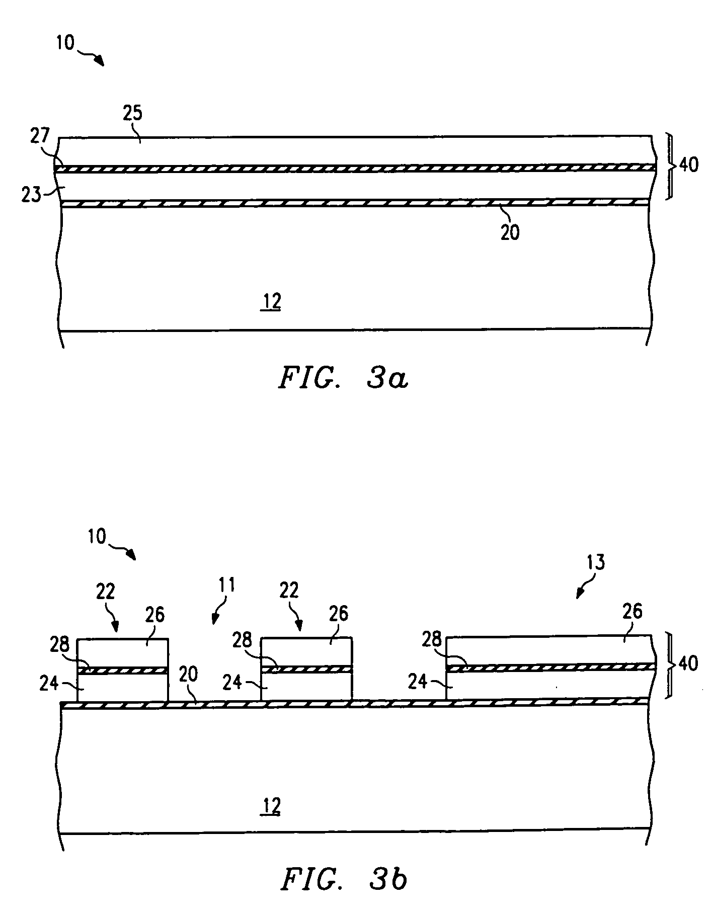
[0017]FIG. 1 is a cross-sectional view of a portion of an integrated circuit 10 having independently formed array and peripheral isolation dielectric regions according to the teachings of the present invention. Integrated circuit 10 comprises a semiconductor substrate 12. A first dielectric layer 20 may be disposed outwardly from an array region 11 of integrated circuit 10. A peripheral dielectric layer 60 may be disposed outwardly from a peripheral region 13 of integrated circuit 10. First dielectric layer 20 and peripheral dielectric layer 60 may comprise, for example, layers of oxide. Other dielectric materials besides oxide may be used to form first and peripheral dielectric layers 20 and 60. First dielectric layer 20 may form a tunnel oxide layer for a floating gate array of memory cells subsequently formed in array region 11. Peripheral dielectric layer 60 may form a gate oxide layer for peripheral transistors subsequently formed in peripheral region 13.

[0018]Gate stacks 22 ar...


PUM


Abstract

The invention comprises a method of forming an integrated circuit, the method comprising: (1) forming a first dielectric layer disposed outwardly from a semiconductor substrate; (2) forming a first intermediate structure outwardly from the a dielectric layer, the first intermediate structure comprising a floating gate layer disposed outwardly from the first dielectric layer, a second dielectric layer disposed outwardly from the floating gate layer, and a first polysilicon layer disposed outwardly from the second dielectric layer; (3) removing regions of the first intermediate structure to form at least one gate stack disposed outwardly from the first dielectric layer; and (4) forming at least one dielectric isolation region after the formation of the gate stacks, wherein the at least one dielectric isolation region is disposed between two gate stacks.

Description

CROSS REFERENCE TO PRIOR APPLICATIONS[0001]This application is a division of Ser. No. 09 / 168,047, filed Oct. 7, 1998 now U.S. Pat. No. 6,194,267 which claims priority based on Provisional Application Ser. No. 60 / 060,561, filed Sep. 30, 1997.TECHNICAL FIELD OF THE INVENTION[0002]This invention relates generally to the field of electronic devices, and more particularly, to an integrated circuit having independently formed array and peripheral isolation dielectrics.BACKGROUND OF THE INVENTION[0003]One type of modern nonvolatile memory is the EPROM or EEPROM device that uses floating gate structures. These floating gate memory structures may be integrated into a floating gate array which facilitates interface between the memory cells, control circuitry and high-voltage power sources. The memory cells use channel hot electrons for programming from the drain side and use Fowler-Nordheim tunneling for erasure from the source side. Due to the high voltages frequently used to program and era...

Claims


Application Information

Patent Timeline
Patent Type & Authority Patents(United States)
IPC IPC(8): H01L29/788H01L27/115H01L21/762H01L21/8247
CPCH01L21/76224H01L27/105H01L27/11521H01L29/7881H01L27/11531H01L27/11534H01L27/11526H10B41/43H10B41/42H10B41/40H10B41/30
Inventor KAYA, CETIN
Owner TEXAS INSTR INC
Why Eureka
Try Eureka