High precision optoelectronic components

a technology of optoelectronic components and components, applied in the field of high-precision optoelectronic components, can solve the problems of large number of components required in the deployment of fiber for these types of applications, sensitive to the cost of e-o-e terminal conversion devices and supporting circuitry, and the cost of both active and passive fiber components and connectorized cables

Active Publication Date: 2007-12-25
SENKO ADVANCED COMPONENTS
View PDF31 Cites 34 Cited by
  • Summary
  • Abstract
  • Description
  • Claims
  • Application Information

AI Technical Summary

Benefits of technology

[0059]In another aspect of the present invention, the components of the optoelectronic assembly are designed for manufacturability by a forming process. In one embodiment, ferrules having two or more points are produced by a forming process on a single sheet work piece. In some embodiments, the ferrule has a star shape. When inserted into a complementary sleeve, the points contact the inner surface of a sleeve to facilitate guiding the optical fibers relative to each other. In another embodiment, a sleeve is produced by a forming process on a single sheet work piece.

Problems solved by technology

The number of components required in the deployment of fiber for these types of applications is large.
In these short distance systems, fiber optics “prove-in” is very sensitive to the cost of E-O-E terminal conversion devices and supporting circuitry, as well as any passive and active optoelectronic devices and equipment linked between terminal ends.
A significant element of the cost of both active and passive fiber components and connectorized cable is the fiber connector itself.
Ferrules and associated means for aligning them (e.g., split sleeves for single fiber connection, ground pins for multi-fiber connections) dominate the cost of current fiber connectors.
It is generally accepted that current fiber connectors cost too much to manufacture.
Stamping processes, however, have not been effective in producing parts With acceptable tolerances for optoelectronic components.
However, Balliet does not provide an enabling disclosure of such stamping process, let alone an enabling disclosure of a stamping process for producing parts within 1000 nm.
Statistically, this means that at most only 3.4 parts per million will not meet dimensional requirements defined by the 1,000 nm tolerance band.

Method used


Image

  • High precision optoelectronic components
  • High precision optoelectronic components
  • High precision optoelectronic components

Examples


Embodiment Construction

[0062]This invention is described below in reference to various embodiments with reference to the figures. While this invention is described in terms of the best mode for achieving this invention's objectives, it will be appreciated by those skilled in the art that variations may be accomplished in view of these teachings without deviating from the spirit or scope of the invention.

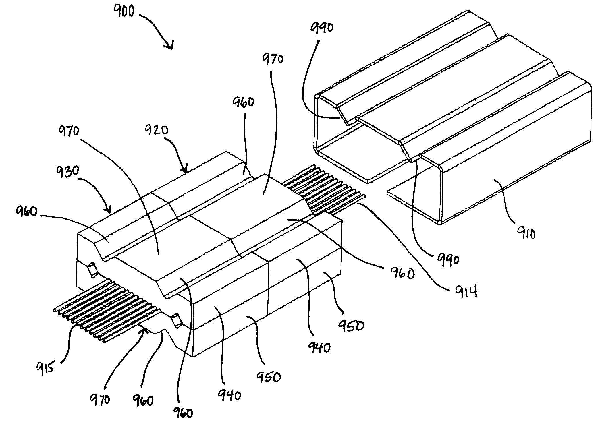
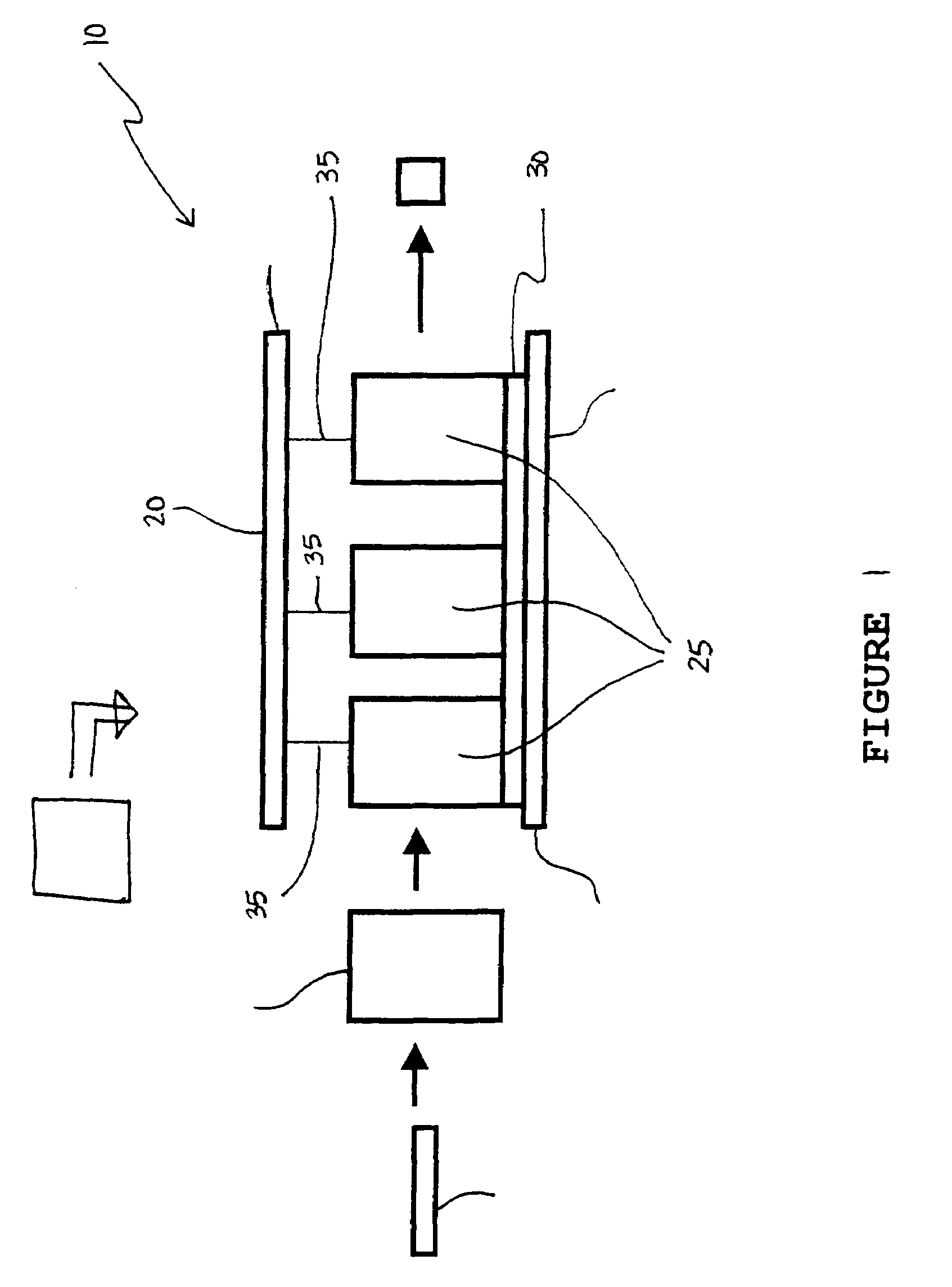
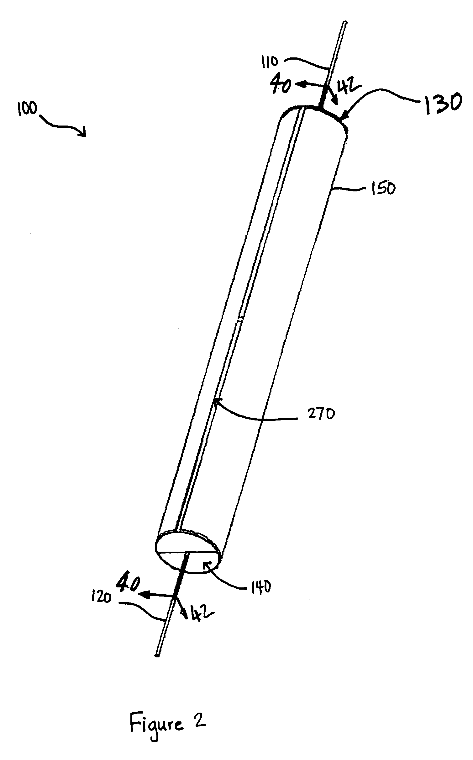
[0063]The present invention is directed to a high precision optical fiber connector for aligning and coupling optical fibers together. The optical fiber connector includes high precision components for supporting and precisely aligning the optical fibers for interconnection. The components of the optical fiber connector are designed so that they can be manufactured by a high-speed stamping system and process capable of producing parts having tolerances below 1000 nm. For purposes of illustrating the principles of the present invention and not by limitation, the present invention is described by reference t...


PUM


Abstract

An optoelectronic assembly having components designed to be fabricated on a stamping process capable of producing parts having tolerances below 1000 nanometers. The optoelectronic assembly includes ferrules and sleeves. The ferrules can include two identical half ferrules that are forged and assembled together to form the ferrule body. The ferrules can also be designed to be alternatively produced by forming processes or produced by a combination of forging and forming processes. The pair of ferrules supporting one or more optical fibers are guided together by a high precision split sleeve for coupling the fibers together.

Description

CROSS-REFERENCE[0001]This application claims priority of the following: (a) U.S. Provisional Patent Application No. 60 / 403,925, filed on Aug. 16, 2002; (b) U.S. Provisional Patent Application No. 60 / 403,926, filed on Aug. 16, 2002; (c) U.S. Provisional Patent Application No. 60 / 403,924, filed on Aug. 16, 2002; and (d) U.S. patent application Ser. No. 10 / 620,851, filed on Jul. 15, 2003. These applications are fully incorporated by reference as if fully set forth herein.BACKGROUND OF THE INVENTION[0002]1. Field of the Invention[0003]The present invention relates to optoelectronic assemblies, sub-assemblies and components, and more particularly to high tolerance components used to align optical fibers in single fiber and multi-fiber optical fiber connections.[0004]2. Description of Related Art[0005]Optical fiber based communication channels are the system of choice in many defense and commercial applications because of their high performance and small size. Particularly, fiber optics h...

Claims


Application Information

Patent Timeline
Patent Type & Authority Patents(United States)
IPC IPC(8): G02B6/36G02B6/38
CPCG02B6/3834G02B6/3885G02B6/3855G02B6/3839G02B6/3636G02B6/3652G02B6/3877
Inventor BARNOSKI, MICHAEL KLEVI, ANTHONYPRINZ, FRITZTARASYUK, ALEX
Owner SENKO ADVANCED COMPONENTS
Why Eureka
Try Eureka