Bridge connection type of chip package and fabricating method thereof

a bridge connection and chip package technology, applied in the direction of electrical apparatus, semiconductor/solid-state device details, semiconductor devices, etc., can solve the problems of signal reflection and signal decay, and achieve the effect of shortening the electrical connection and improving the electrical performance of the packag

Inactive Publication Date: 2007-12-25
ADVANCED SEMICON ENG INC
View PDF18 Cites 2 Cited by
  • Summary
  • Abstract
  • Description
  • Claims
  • Application Information

AI Technical Summary

Benefits of technology

[0008]Accordingly, one object of the present invention is to provide a chip package structure and fabricating method thereof capable of shortening the electrical connections between a chip and a substrate so that electrical performance of the package is improved.
[0017]In brief, the chip contact on the chip and the substrate contact on the substrate are electrically connected to each other directly or indirectly through a conductive trace. Hence, the transmission path between the chip contact and the substrate contact is shortened and the transmission section is widened. Consequently, transmission impedance and signal decay are reduced. Thus, the package is suitable for high frequency operation because there is considerable reduction in parasitic inductance and capacitance. Moreover, since the substrate contact and the chip contact are in direct contact or through a conductive trace having a relatively large contact area with both the substrate contact and the chip contact, impedance mismatch commonly present in a wire bonding connection can be prevented. Ultimately, electrical performance of the package is improved.

Problems solved by technology

Since a conductive wire has a relatively small cross-sectional area and long length, resistant mismatch often results in signal decay.
At high-frequency signaling operation, in particular, parasitic induction-capacitance in the wire may result in signal reflection.

Method used


Image

  • Bridge connection type of chip package and fabricating method thereof
  • Bridge connection type of chip package and fabricating method thereof
  • Bridge connection type of chip package and fabricating method thereof

Examples


Embodiment Construction

[0030]Reference will now be made in detail to the present preferred embodiments of the invention, examples of which are illustrated in the accompanying drawings. Wherever possible, the same reference numbers are used in the drawings and the description to refer to the same or like parts.

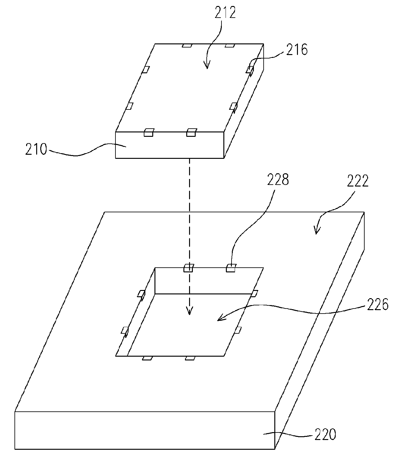
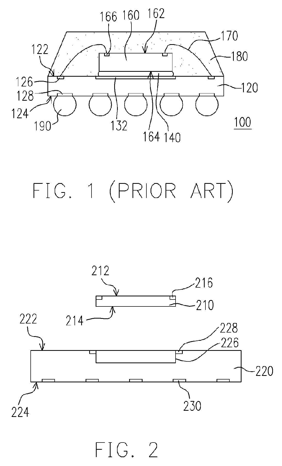
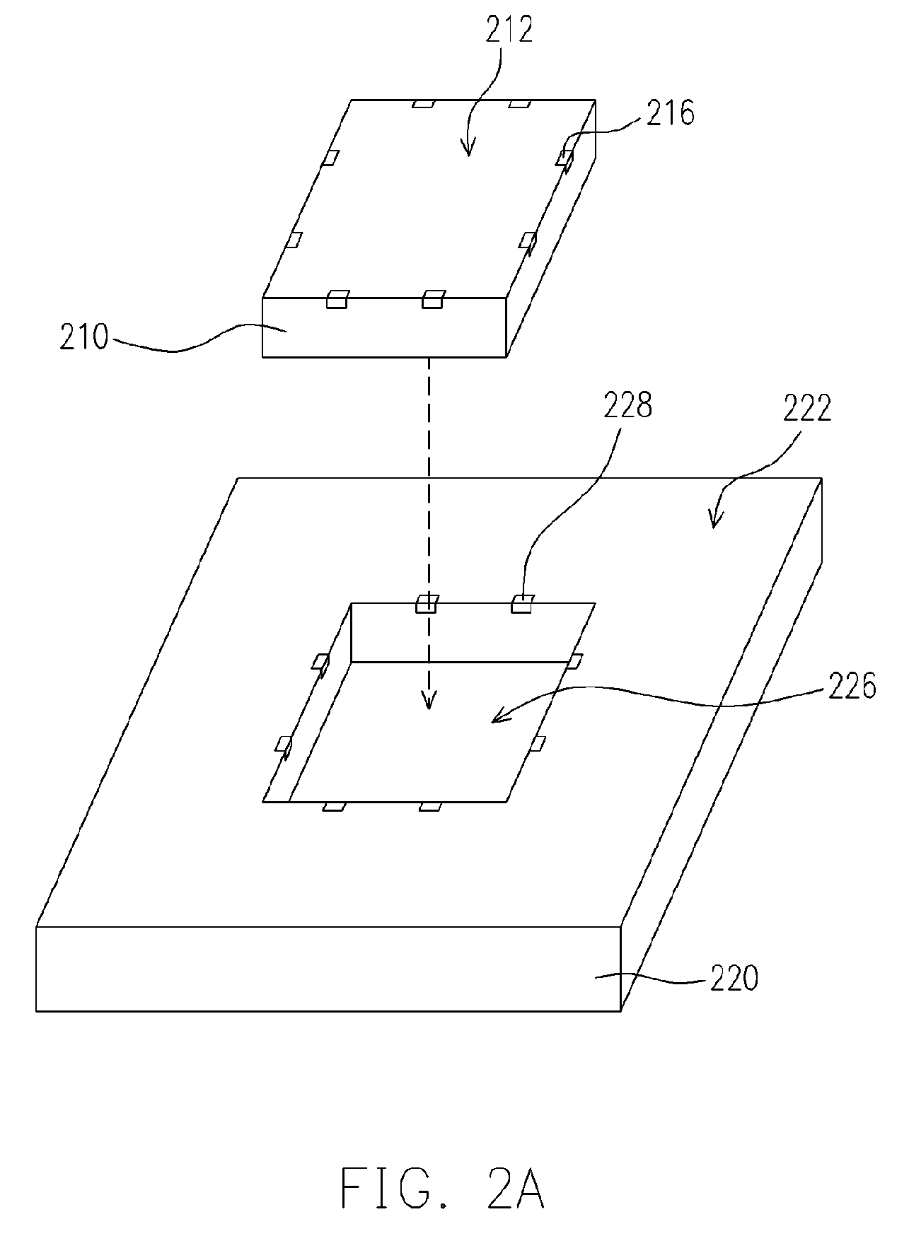
[0031]FIGS. 2 to 7 are cross-sectional views showing the progression of steps for fabricating a chip package according to a first preferred embodiment of this invention. FIG. 2A is a perspective view of the chip and the substrate in FIG. 2. To fabricate a chip package, a chip 210 and a substrate 220 having a first surface 222 and a second surface 224 are provided as shown in FIGS. 2 and 2A. The substrate 226 has cavity 226 and a plurality of substrate contacts 228, 230 on the first surface 222 of the substrate 220. The substrate contacts 228 are on the edges surrounding the cavity 226. That is, the substrate contacts 228 are located next to the opening edges of the cavity 226. The chip 210 has an act...


PUM


Abstract

A chip package having at least a substrate, a chip and a conductive trace is provided. The substrate has a first surface, a second surface, a cavity and at least one substrate contact all positioned on the first surface of the substrate. The chip has an active surface with at least one chip contact thereon. The chip is accommodated inside the cavity with at least one sidewall having contact with one of the sidewalls of the cavity. The active surface of the chip and the first surface of the substrate are coplanar. The conductive trace runs from the active surface of the chip to the first surface of the substrate so that the chip contact and the substrate contact are electrically connected.

Description

CROSS-REFERENCE TO RELATED APPLICATION[0001]This application is a divisional of a prior application Ser. No. 10 / 250,290, filed on Jun. 20, 2003, now U.S. Pat. No. 6,833,610 which claims the priority benefit of Taiwan application serial no. 91123066, filed on Oct. 7, 2002.BACKGROUND OF THE INVENTION[0002]1. Field of Invention[0003]The present invention relates to a type of chip package and fabricating method. More particularly, the present invention relates to a bridge connection type of chip package and fabricating method thereof for improving electrical performance.[0004]2. Description of Related Art[0005]Accompanying the rapid progress in electronic technologies, more personalized and functionally powerful electronic products are developed. To facilitate use and enhance portability, most electronic products are designed to have a lighter weight and a smaller size. Whether a given electronic product can be miniaturized depends largely on the size of the chip package embedded inside...

Claims


Application Information

Patent Timeline
Patent Type & Authority Patents(United States)
IPC IPC(8): H01L21/00H01L21/60H01L23/498H01L23/538
CPCH01L23/49816H01L24/24H01L24/82H01L23/5389H01L2924/01033H01L2224/24227H01L2224/32225H01L2224/48091H01L2224/48227H01L2224/73265H01L2924/01082H01L2924/15153H01L2924/15165H01L2924/15311H01L2924/30105H01L2924/30107H01L2924/3011H01L24/48H01L2924/01047H01L2924/014H01L2924/10253H01L2924/00014H01L2924/00H01L2924/00012H01L24/73H01L2924/00015H01L2924/181H01L2224/45099H01L2224/05599H01L2224/85399H01L2224/45015H01L2924/207
Inventor HUNG, CHIH-PIN
Owner ADVANCED SEMICON ENG INC
Why Eureka
Try Eureka