Photomask producing method and photomask blank

a technology of photomask and producing method, which is applied in the field of photomask producing method and photomask blank, can solve the problems of variation in cd accuracy, particularly difficult control of etching progress directivity, and difficulty in cd accuracy variation, so as to reduce the damage to the surface of the chromium film, reduce the problem, and reduce the loading effect

Active Publication Date: 2008-01-01
HOYA CORP +1
View PDF11 Cites 10 Cited by
  • Summary
  • Abstract
  • Description
  • Claims
  • Application Information

AI Technical Summary

Benefits of technology

[0018]Specifically, a first object of this invention is to provide a method that can suppress the loading effect and achieve a high CD accuracy when forming a highly accurate pattern by dry etching, in a photomask having a global opening ratio difference (variation in CD accuracy due to the loading effect becomes a problem).
[0067]Particularly, in the halftone-type phase shift mask and the chromeless-type phase shift mask, the use of the inorganic-based etching mask achieves reduction in loading effect, and further, the inorganic-based etching mask functions as a protective layer for the chromium film when etching the phase shift layer or the substrate. Therefore, damage to the surface of the chromium film is decreased so that it is possible to remarkably diminish the problem that particles generated thereby are transferred due to etching of the phase shift material layer and remain as a pattern defect.

Problems solved by technology

However, with respect to the demand for higher accuracy of the patterns of the photomasks following the high integration of the semiconductor integrated circuits and so forth, it has become clear that the current method of forming a pattern from a chromium-based opaque film by using a resist pattern as an etching mask raises a problem of variation in CD (critical dimension) accuracy due to the loading effect in connection with a photomask wherein pattern regions having a global opening ratio difference are compositely present in the mask plane.
For example, when resist patterns having the same dimensions are formed in respective regions having an opening ratio difference in opaque pattern so as to form chromium-based opaque film patterns of the same dimensions, respectively, there arises a problem that the respective opaque patterns formed by dry etching using the resist patterns of the same dimensions as masks exhibit different dimensions due to the difference between the opening ratios in the respective regions by the so-called loading effect to thereby cause variation in CD accuracy.
There is a problem that since contribution of radicals is large in this etching reaction, the etching progress directivity is particularly difficult to control.
H8-234410, there is a problem that when local inequality exists in the pattern opening ratio (i.e. when pattern regions with different densities compositely exist), it is complicated to provide an adjusting pattern corresponding thereto and it is difficult to cope with high integration of semiconductor integrated circuits.
Further, since it is necessary to form the pattern that is not normally required, an increase in pattern data amount used in production of a photomask can not be avoided.
This becomes a large problem in producing semiconductor devices with extremely high integration in recent years.
However, in order to suppress the loading effect and to achieve the high CD accuracy under the circumstances where the finer formation of the patterns and the differences in density of the patterns are in progress as described above, it is insufficient to merely use the hard mask and further technological improvement is required.
H10-69055, since the chromium-based opaque film requires a prescribed opaque property (e.g. OD (optical density) of 3.0 or more), there is a limit to reduction in thickness of the opaque film, and resultantly, there is also a limit to reduction in thickness of the resist, and therefore, there is a limit to improvement in CD accuracy.
On the other hand, there is also a problem that, depending on the etching condition of the phase shift material layer, the surface of the chromium-based opaque film is damaged on etching of the phase shift material layer, and particles generated thereby affect the etching of the phase shift material layer and remain as a pattern defect, which thus narrows the width of selection in etching condition.

Method used


Image

  • Photomask producing method and photomask blank
  • Photomask producing method and photomask blank
  • Photomask producing method and photomask blank

Examples


first embodiment

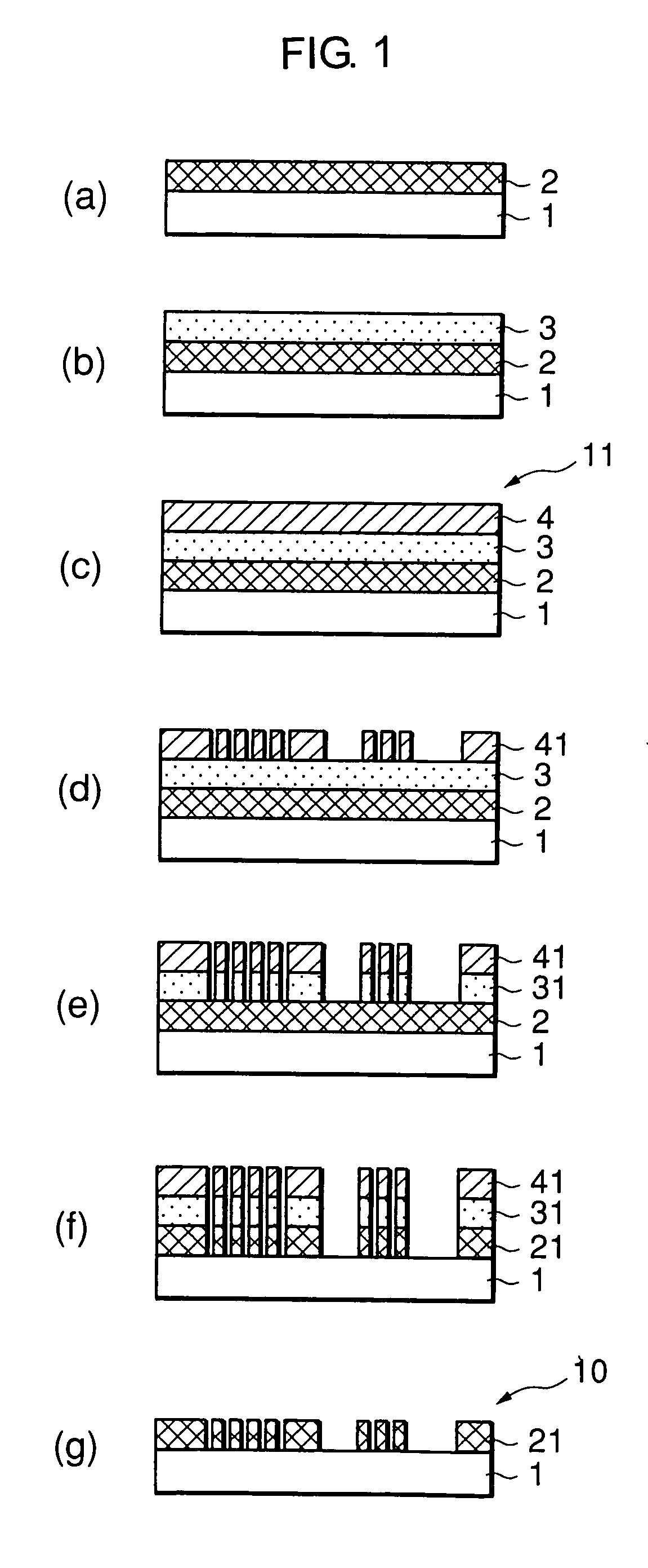
[0072]Referring to FIG. 1, description will be made of a photomask producing method according to the first embodiment of this invention.

[0073]First, a substrate made of quartz was mirror-polished and was subjected to prescribed washing to thereby obtain a light-transmissive substrate 1 of 6 inches×6 inches×0.25 inches.

[0074]Then, by the use of an in-line sputtering apparatus where a plurality of chromium (Cr) targets were disposed in the same chamber, an opaque chromium film 2 was formed on the light-transmissive substrate 1 (see FIG. 1(a)).

[0075]Specifically, first, reactive sputtering was carried out in an atmosphere of mixture gas of argon (Ar) and nitrogen (N2) (Ar:N2=72:28 [volume %], pressure 0.3 [Pa]) to thereby form a CrN film having a thickness of 20 [nm].

[0076]Subsequently, reactive sputtering was carried out in an atmosphere of mixture gas of argon (Ar) and methane (CH4) (Ar:CH4=96.5:3.5 [volume %], pressure 0.3 [Pa]) to thereby form a CrC film having a thickness of 37 [n...

second embodiment

[0089]Referring to FIG. 1, description will be made of a photomask producing method according to the second embodiment of this invention. In the second embodiment, a photomask was produced under the same condition as in the first embodiment except that the opaque chromium film 2 was etched using only the inorganic-based etching mask pattern 31 as a mask after removal of the resist pattern 41 in the first embodiment.

[0090]Specifically, first, a substrate made of quartz was mirror-polished and was subjected to prescribed washing to thereby obtain a light-transmissive substrate 1 of 6 inches×6 inches×0.25 inches.

[0091]Then, by the use of an in-line sputtering apparatus where a plurality of chromium (Cr) targets were disposed in the same chamber, an opaque chromium film 2 was formed on the light-transmissive substrate 1 (see FIG. 1(a)).

[0092]Specifically, first, reactive sputtering was carried out in an atmosphere of mixture gas of argon (Ar) and nitrogen (N2) (Ar:N2=72:28 [volume %], p...

third embodiment

[0115]Referring to FIG. 3, description will be made of a photomask producing method according to the third embodiment of this invention.

[0116]First, a substrate made of quartz was mirror-polished and was subjected to prescribed washing to thereby obtain a light-transmissive substrate 1 of 6 inches×6 inches×0.25 inches.

[0117]Then, by the use of a mixture target of molybdenum (Mo) and silicon (Si) (Mo:Si=20:80 [mol %]), reactive sputtering was carried out in an atmosphere of mixture gas of argon (Ar) and nitrogen (N2) (Ar:N2=10:90 [volume %], pressure 0.3 [Pa]) to thereby form an MoSiN-based light-semitransmissive phase shift film 5 having a thickness of 100 [nm] on the light-transmissive substrate 1 (FIG. 3(a)).

[0118]Then, by the use of an in-line sputtering apparatus where a plurality of chromium (Cr) targets were disposed in the same chamber, an opaque chromium film 2 comprised of a CrN film, a CrC film, and a CrON film was formed on the phase shift film 5 according to the same met...


PUM

PropertyMeasurementUnit
widthaaaaaaaaaa
widthaaaaaaaaaa
widthaaaaaaaaaa

Abstract

In a method of producing a photomask (10) in which a light-transmissive substrate (1) is formed thereon with a chromium pattern (21) having a global opening ratio difference in its plane on the light-transmissive substrate (1), use is made, as an etching mask for a chromium film (2), of an etching mask pattern (31) made of an inorganic-based material having a resistance against etching of the chromium film (2). Dry etching of the chromium film (2) is carried out under a condition selected from conditions that cause damage to a resist pattern (41) to a degree which is unallowable when etching the chromium film (2) using the resist pattern (41) as a mask.

Description

[0001]This application claims priority to Japanese Patent Application No. 2003-105921 Apr. 9, 2003, the disclosure of which is incorporated herein by reference.BACKGROUND OF THE INVENTION[0002]This invention relates to a method of producing a photomask for use in production of a semiconductor integrated circuit, a liquid crystal display device, or the like, and to a photomask blank for use therein.[0003]Following high integration of semiconductor integrated circuits, liquid crystal display devices, etc., and so forth, there has been an increasing demand for high pattern accuracy with respect to photomasks that are used in fine processing during the production process thereof.[0004]In the photomasks currently used, a pattern formed by an opaque film is provided on a transparent substrate, and a chromium-based material is generally used as the opaque film in terms of processability of a highly accurate pattern.[0005]However, with respect to the demand for higher accuracy of the patter...

Claims


Application Information

Patent Timeline
Patent Type & Authority Patents(United States)
IPC IPC(8): G03F1/00G03C5/00G03F1/32G03F1/34G03F1/68G03F1/80G03F9/00H01L21/027H01L21/3065
CPCG03F1/80G03F1/32G03F1/34G03F1/46G03F1/76H01L21/027H01L21/0273H01L21/30655
Inventor OKUBO, YASUSHIHARA, MUTSUMI
Owner HOYA CORP
Why Eureka
Try Eureka