Molded leadless package having a partially exposed lead frame pad

a lead frame pad and partially exposed technology, applied in the field of silicone package, can solve the problems of affecting the stability and reliability of the silicone package and the chip it contains, adversely affecting their reliability, and it is not easy to extend the length of the hygroscopic path into the mlps, so as to improve reliability and increase thermal transferability

Active Publication Date: 2008-01-01
SEMICON COMPONENTS IND LLC
View PDF11 Cites 107 Cited by
  • Summary
  • Abstract
  • Description
  • Claims
  • Application Information

AI Technical Summary

Benefits of technology

[0018]The present invention provides an MLP having a modified structure in which a portion of a lead frame pad is exposed in order to achieve improved reliability and increased thermal transferability.
[0020]The present invention also provides a sawing type MLP which improves the reliability of a system package, and a method of manufacturing the same.
[0021]The present invention also provides a sawing type MLP which is less susceptible to collapsing or tilting during the process of manufacturing a system package, and a method of manufacturing the same.
[0044]According to the present invention, the lower surface of the die pad is on the same plane as the bottoms of the leads. However, since the short-circuit preventing member with a predetermined height is attached on the lower surface of the die pad, the likelihood of a short-circuit between the die pad and circuit lines on a system board is substantially reduced. The height of the short-circuit preventing member may be more than 30 μm, and preferably more than 50 μm. Thus, the reliability of a solder joint coupling the leads to the system board is improved.

Problems solved by technology

Thus, the transferability of heat generated from a semiconductor chip inside a semiconductor package via an external board greatly affects the stability and reliability of the semiconductor package and the chip it contains.
However, the above-described conventional MLPs have certain features that may adversely impact their reliability.
Also, it is not easy to extend the length of a hygroscopic path into the MLPs.
This movement may cause the solder joint 16 to flow to one side or the other, and thus the height h1 of the solder joint 16 may be difficult to control or secure.
As a result, the reliability of the MLP 1100 may be adversely affected by, for example, a die pad 1130 contacting and / or electrically shorting to a circuit line 14 of the system board 10.
Further, the sensitivity of solder joint 16 to thermal and / or mechanical stress is significantly increased and the reliability of the system package may be adversely affected if the height h1 of the solder joint 16 is less than the desired minimum and / or insufficient.
Moreover, the reliability of the system package may be adversely affected by the MLP 1100 tilting or collapsing such that one or more leads 1140 come into direct contact with corresponding coupling pads 12 due to movement of the solder joint 16 during mounting of the MLP 1100 on the system board 10.

Method used


Image

  • Molded leadless package having a partially exposed lead frame pad
  • Molded leadless package having a partially exposed lead frame pad
  • Molded leadless package having a partially exposed lead frame pad

Examples


Embodiment Construction

[0098]The present invention will now be described in more detail with reference to the accompanying drawings in which exemplary embodiments of the present invention are shown. The invention may, however, be embodied in many different forms and should not be construed as being limited to the embodiments set forth herein.

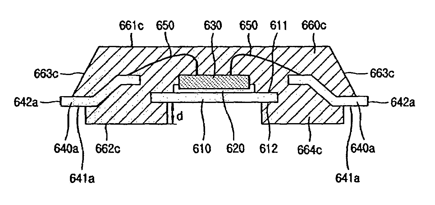
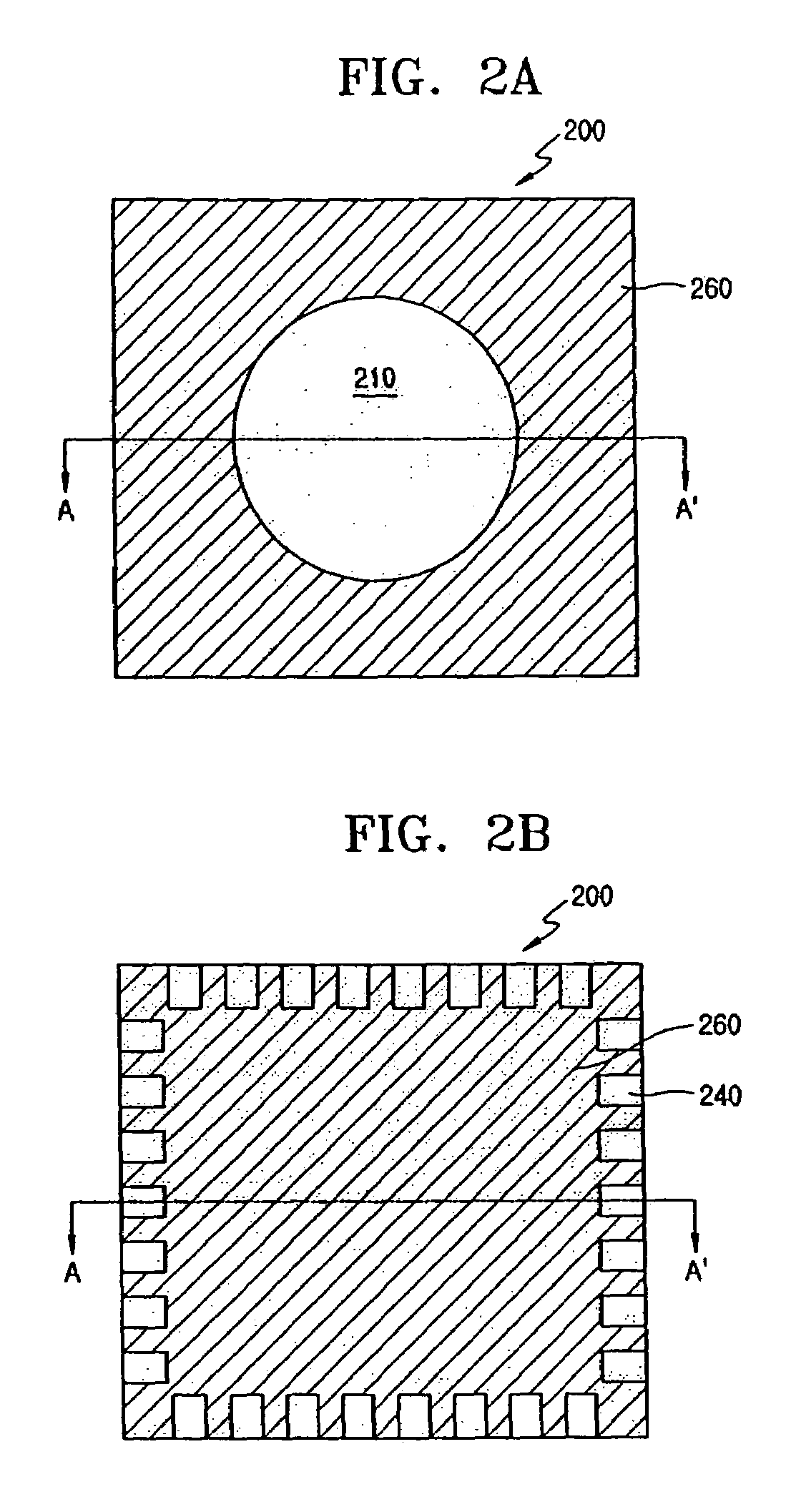
[0099]FIGS. 2A and 2B are a plan view and a rear view, respectively, of an MLP according to one embodiment of the present invention.

[0100]Referring to FIGS. 2A and 2B, an MLP 200 includes a lead frame pad 210 including an upper surface having a central portion thereof exposed by a molding material 260. The exposed portion of the lead frame pad 210 is, in this embodiment, generally circular in shape. The MLP 200 also includes leads 240 each of which include a lower surface having an edge exposed by the molding material 260. In other words, a plurality of leads 240 is spaced apart from one another at the edge of the molding material 260. As is described more particularl...


PUM


Abstract

Provided are a molded leadless package, and a sawing type molded leadless package and method of manufacturing same. The molded leadless package includes a lead frame pad having first and second surfaces opposite to each other. A semiconductor chip is adhered to the first surface of the lead frame pad. A lead is electrically coupled to the semiconductor chip. A molding material covers the lead frame pad, the semiconductor chip, and the lead and exposes a portion of the lead and a portion of the second surface of the lead frame pad. A step difference is formed between a surface of the molding material covering the second surface of the lead frame pad and the second surface of the lead frame pad itself. The sawing type molded leadless package includes a short-circuit preventing member that is post-shaped or convex, and protruding from the lower surface of the die pad.

Description

BACKGROUND OF THE INVENTION[0001]This application claims the priorities of Korean Patent Application No. 2003-0080143, filed on Nov. 13, 2003, No. 2004-0060691, filed on Jul. 31, 2004 and No. 2004-0071789, filed on Sep. 8, 2004, in the Korean Intellectual Property Office, the disclosures of which are incorporated herein in their entireties by reference.[0002]1. Field of the Invention[0003]The present invention relates to a semiconductor package and, more particularly, to a molded leadless package (MLP) having improved reliability and high thermal transferability. Further, the present invention relates to MLPs singulated by stamping / punching and by sawing, and a method of manufacturing the same.[0004]2. Description of the Related Art[0005]In general, semiconductor packages are packages in which semiconductor chips are mounted on and / or connected to a lead frame. As the semiconductor chip is operated, and / or a voltage of predetermined magnitude is applied to an internal element of the...

Claims


Application Information

Patent Timeline
Patent Type & Authority Patents(United States)
IPC IPC(8): H01L23/495H01L23/31H01L23/433
CPCH01L23/4334H01L23/49568H01L24/97H01L23/315H01L23/3107H01L2924/07802H01L2224/32245H01L2224/48091H01L2224/48227H01L2224/48247H01L2224/48465H01L2224/49171H01L2224/73265H01L2224/97H01L2924/01013H01L2924/01029H01L2924/01078H01L2924/01079H01L2924/01082H01L2924/14H01L2924/1815H01L2924/01033H01L2924/01023H01L2924/01006H01L2924/01005H01L24/49H01L24/48H01L2924/00014H01L2224/85H01L2224/83H01L2924/00H01L2924/00012H01L24/73H01L2224/05554H01L2924/12042H01L2924/181H01L2924/351
Inventor CHOI, YOON-HWANAM, SHI-BAEKJEON, O-SEOBJOSHI, RAJEEV DINKARESTACIO, MARIA CRISTINA B.
Owner SEMICON COMPONENTS IND LLC
Why Eureka
Try Eureka