Driving method for electro-optical device, electro-optical device, and electronic apparatus

a technology of electrooptical devices and driving methods, applied in electrical devices, semiconductor devices, instruments, etc., can solve the problems of complicated pixel structure, limited gray-scale level limitation, and non-uniform luminescence state of luminescent elements, and achieve advantageously low power consumption of organic electro-luminescent elements

Inactive Publication Date: 2008-01-01
BOE TECH GRP CO LTD
View PDF36 Cites 222 Cited by
  • Summary
  • Abstract
  • Description
  • Claims
  • Application Information

AI Technical Summary

Benefits of technology

[0018]According to a seventh driving method for an electro-optical device of the present invention, in the above-described driving method for an electro-optical device, the set signal may be a signal to set the driving transistor to the conducting state rather than the signal to select the conducting state or the non-conducting state of the driving transistor. This means that an intermediate conducting state other than the two states, i.e., the conducting state and the non-conducting state, of the driving transistor is selectable. This can be implemented by the set signal provided as a voltage having three or more consecutive or discrete values. This driving method is effective to implement many gray-scale levels.
[0019]According to an eighth driving method for an electro-optical device of the present invention, in the above-described driving method for an electro-optical device, the electro-optical element may be an organic electro-luminescence element. Generally, the power consumption of the organic electro-luminescence element is advantageously low.

Problems solved by technology

When thin-film transistors having different current characteristics are used, however, the difference in the current characteristics of the individual transistors may sometimes directly result in non-uniformity in the luminescence state of the luminescent elements.
In this method, however, the number of gray-scale levels is restricted by the number of sub-pixels.
For a greater number of gray-scale levels, pixels must be divided into a greater number of sub-pixels, which makes the pixel structure complicated.

Method used


Image

  • Driving method for electro-optical device, electro-optical device, and electronic apparatus
  • Driving method for electro-optical device, electro-optical device, and electronic apparatus
  • Driving method for electro-optical device, electro-optical device, and electronic apparatus

Examples


Embodiment Construction

[0037]Preferred embodiments of the present invention are described below.

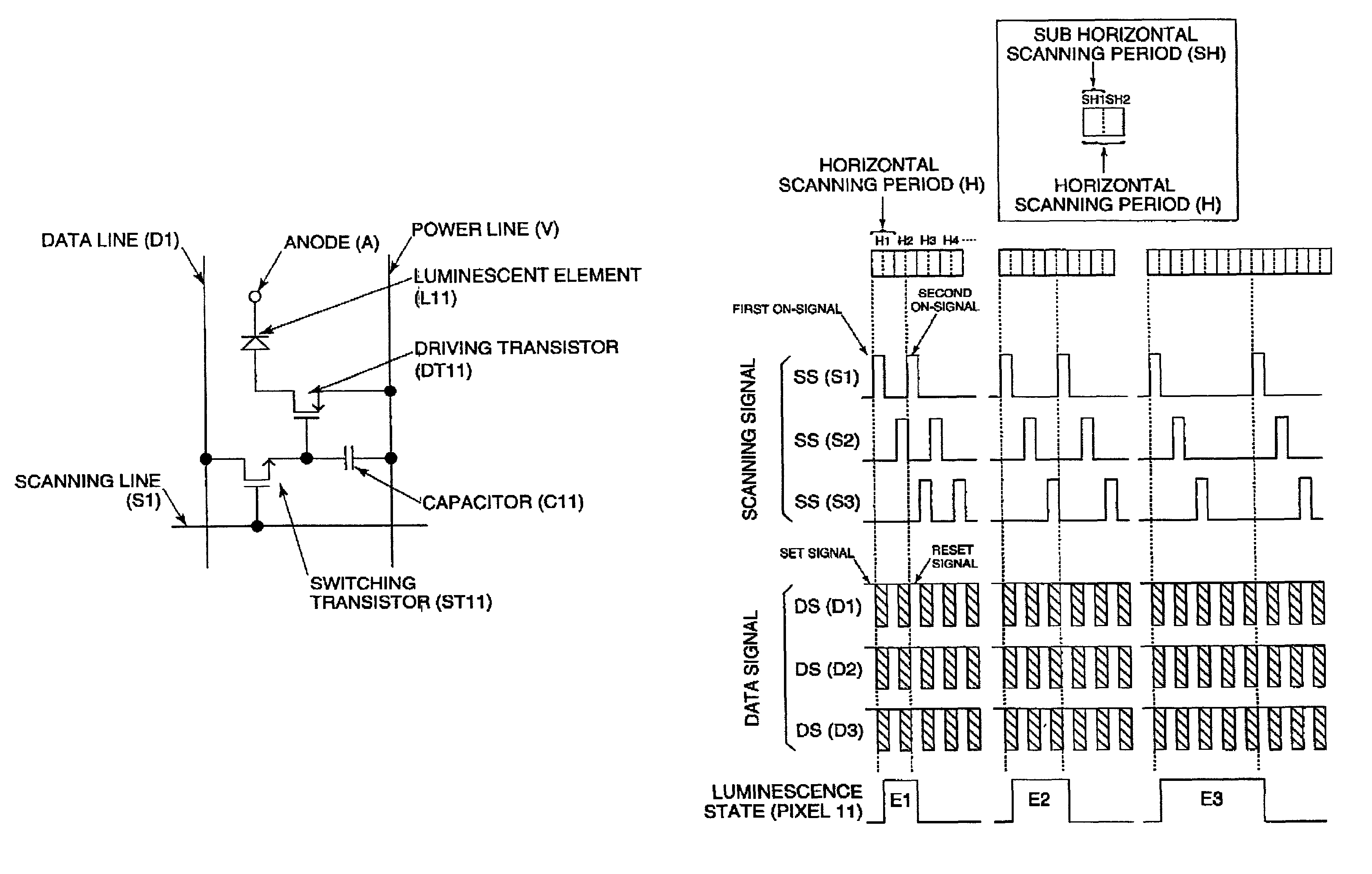
[0038]A basic circuit used in an embodiment of the present invention includes a poly-crystal silicon thin-film transistor formed by a low-temperature process at 600° C. or lower (low-temperature poly-Si TFT). The low-temperature poly-Si TFT can be formed on a large, inexpensive glass substrate, and can integrate a driving circuit on a panel, and accordingly, it is suitable for manufacturing an electro-optical device. Additionally, the low-temperature poly-Si TFT is small, but has a high current supplying power. Accordingly, it is suitable for use in a high-precision current luminescence display device. The present invention is also applicable to an electro-optical device driven by other types of transistors, such as an amorphous silicon thin-film transistor (a-Si TFT), a silicon-based transistor, and an organic thin-film transistor using an organic semiconductor.

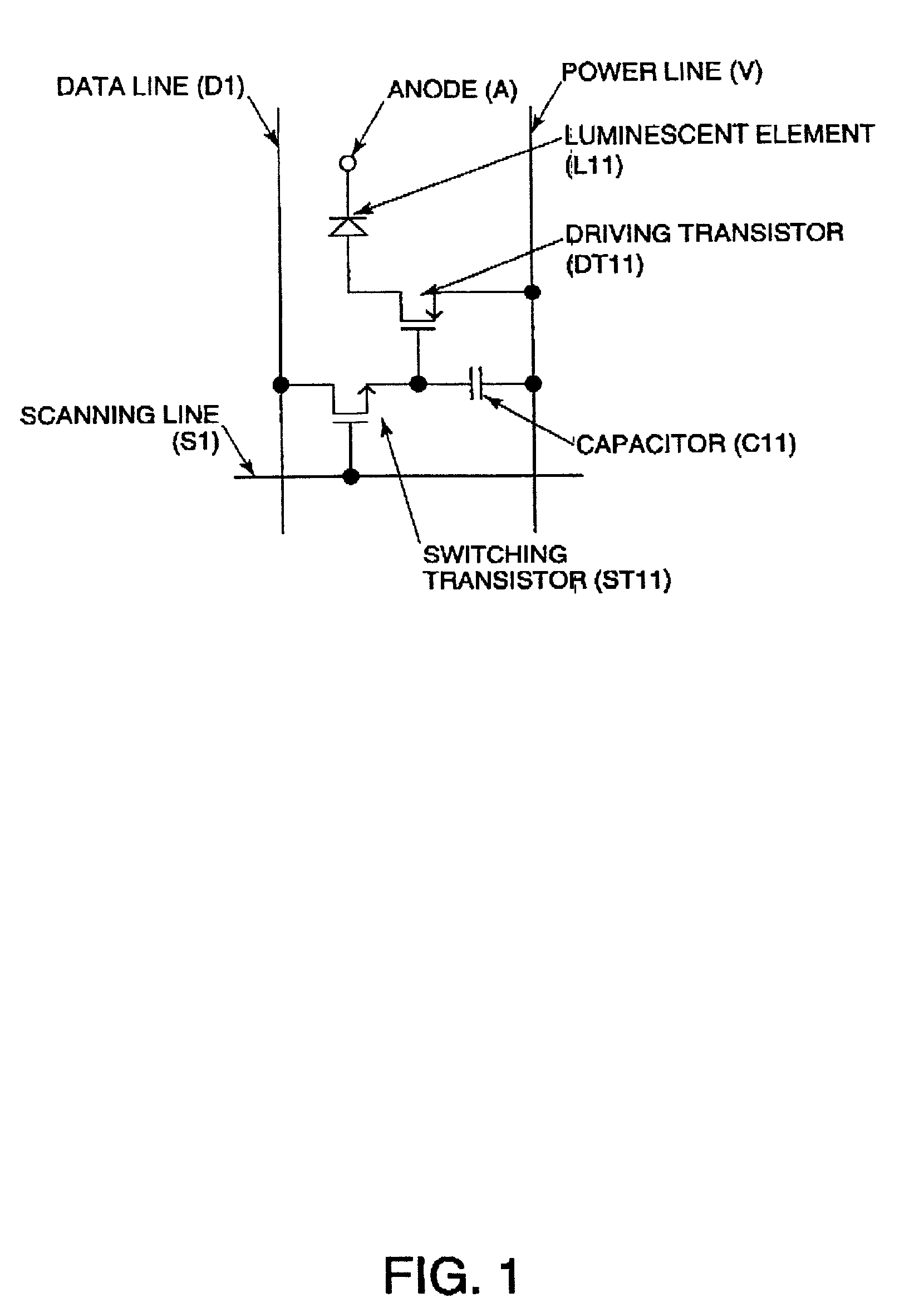
[0039]The equivalent circuit of one pixel of an e...


PUM


Abstract

The invention provides a method for implementing a multi-level display of an electro-optical device according to a time ratio gray-scale method without providing reset lines. In an electro-optical device that includes, at an intersection of a scanning line and a data line, an electro-optical element, a driving transistor that drives the electro-optical element, and a switching transistor that controls the driving transistor, a gray-scale is obtained by performing a plurality of set-reset operations. Each set-reset operation includes: a setting step of supplying an on-signal to the switching transistor via the scanning line, and of supplying a set signal to select a conducting state or a non-conducting state of the driving transistor to the driving transistor via the data line and the switching transistor in accordance with the one signal; and a resetting step of supplying an on-signal to the switching transistor via the scanning line, and of supplying a reset signal to select the non-conducting state of the driving transistor to the driving transistor via the data line and the switching transistor in accordance with the one signal.

Description

BACKGROUND OF THE INVENTION[0001]1. Field of Invention[0002]The present invention relates to a driving method for an organic electro-luminescence display device, a driving method for an electro-optical device suitable for use with an organic electro-luminescence display device the electro-optical device, and an electronic apparatus provided with such an electro-optical device.[0003]2. Description of Related Art[0004]Attention is being given to organic electro-luminescence (electric-field luminescence) display devices using organic materials as luminescent materials of luminescent elements since they have a wide viewing angle, and will potentially meet market demands, i.e., demands for thinner, lighter, smaller, and lower power-consuming display devices.[0005]Unlike conventional liquid crystal display devices, in organic electro-luminescence display devices, the luminescence state of the luminescent element must be controlled by a current. One such control method is the conductance c...

Claims


Application Information

Patent Timeline
Patent Type & Authority Patents(United States)
IPC IPC(8): G09G3/30G09G3/20G09G3/32H01L27/32
CPCG09G3/3258G09G3/20G09G3/2022G09G2300/0417G09G2300/0842H01L27/3244H01L27/3295H10K59/122H10K59/12
Inventor KIMURA, MUTSUMI
Owner BOE TECH GRP CO LTD
Why Eureka
Try Eureka