

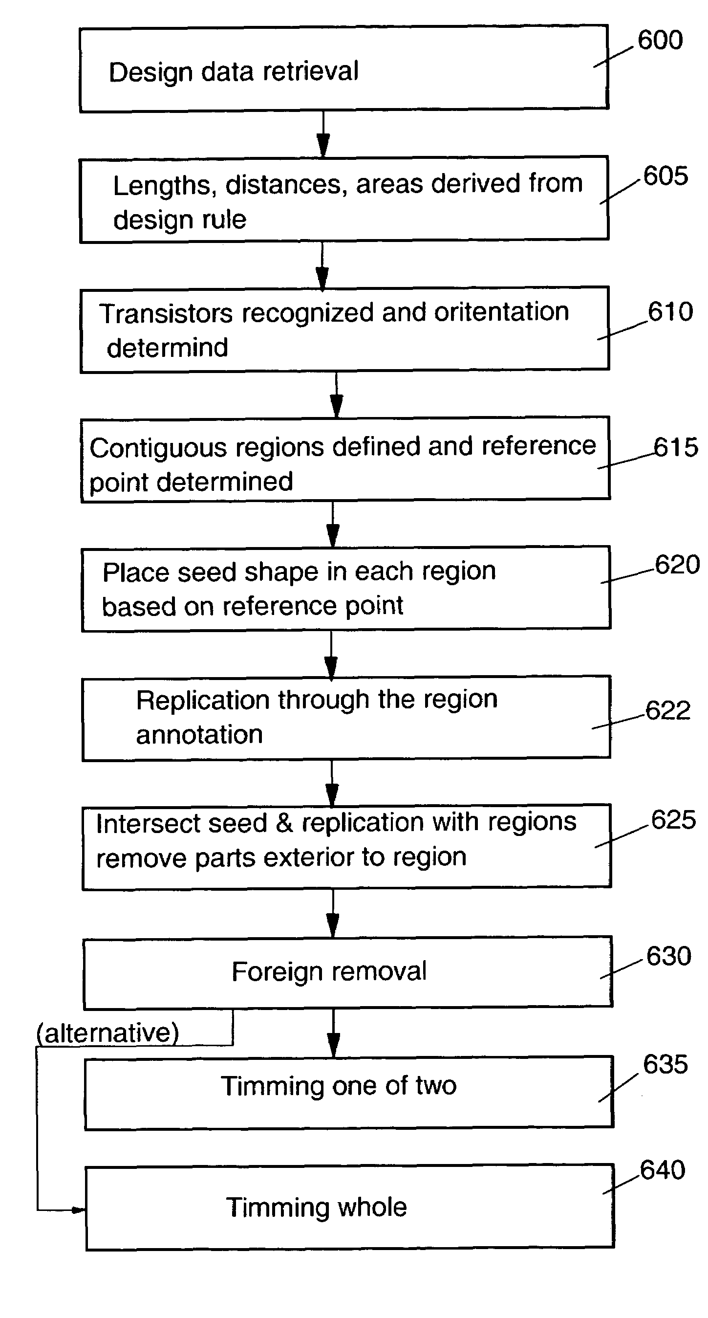
Method and device for automated layer generation for double-gate FinFET designs
a technology of double-gate finfet and automatic layer generation, which is applied in the field of field effect transistors, can solve the problems of affecting the design of existing designs based on non-finfet technology, the formation of said sidewall spacers, and the violation of electronic properties exemplary design rules,
- Summary
- Abstract
- Description
- Claims
- Application Information
AI Technical Summary
Benefits of technology
Problems solved by technology
Method used
Image

Examples
Embodiment Construction
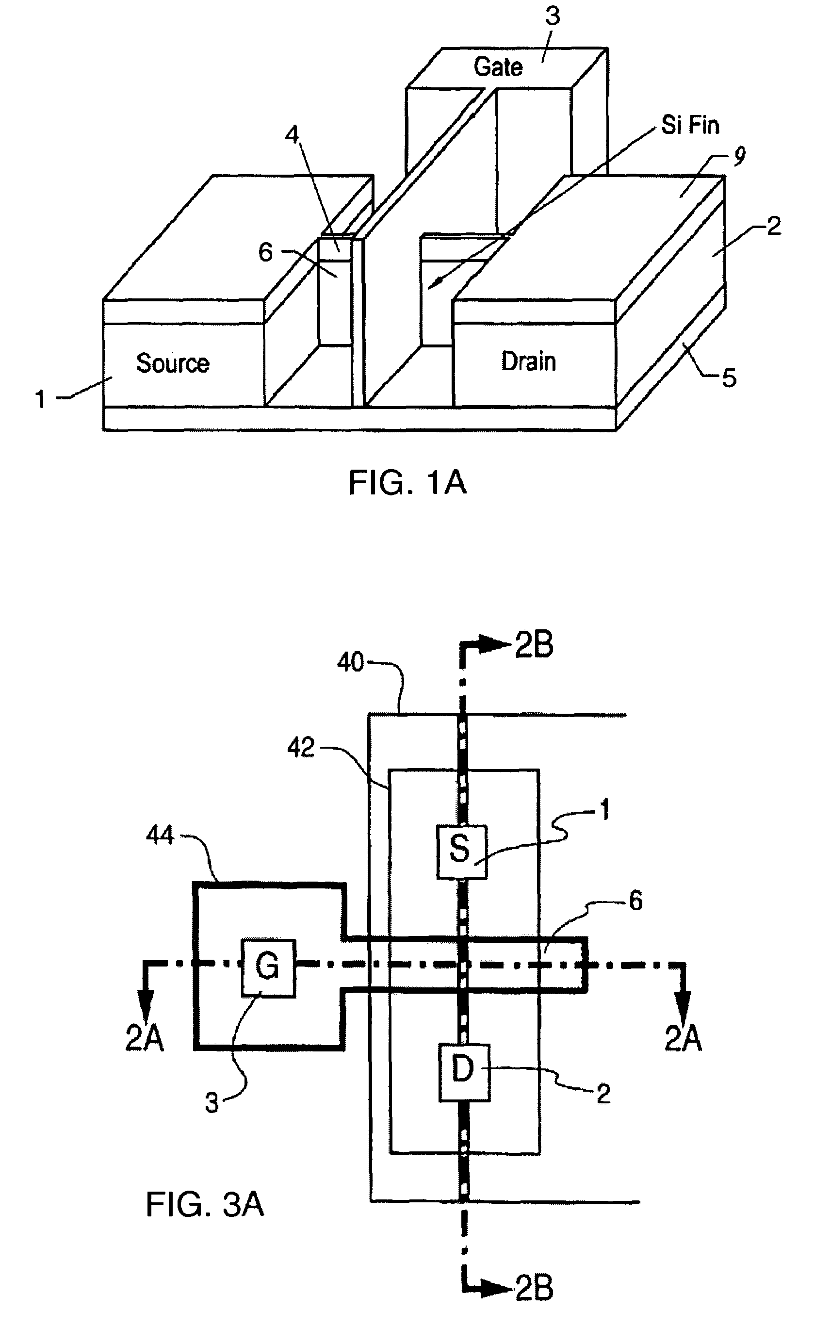
[0032]Referring to the drawing, FIG. 1A illustrates in perspective a typical fin structure (in the present example a FET) in accordance with a known prior art approach. Such a planarized silicon fin device is disclosed e.g. in U.S. Pat. No. 6,252,284 by Paul Muller et al., assigned to the present assignee, issued Jun. 26, 2001. A corresponding double-gated FinFET transistor structure is disclosed e.g. in U.S. Pat. No. 6,413,802 assigned to University of California and issued Jul. 2, 2002.
[0033]In the structure shown in FIG. 1A, the device is fabricated on insulating layer 5, e.g. a Silicon-on-Insulator (SoI) substrate, and includes a silicon drain island 2 and a source island 1 connected by a silicon fin or channel 6. The source, drain and channel are covered by a dielectric layer 9 (hard mask), and a gate 3 extends across the channel fin 4 and is isolated therefrom by gate oxide and the hard mask. The channel 6 extends horizontally on the substrate 5 with the gates in planes on eit...
PUM
| Property | Measurement | Unit |
|---|---|---|
| lengths | aaaaa | aaaaa |
| width | aaaaa | aaaaa |
| cell structure | aaaaa | aaaaa |
Abstract
Description
Claims
Application Information