Light-emitting device, light-emitting apparatus, image display apparatus, method of manufacturing light-emitting device, and method of manufacturing image display apparatus

a technology of light-emitting devices and light-emitting devices, which is applied in the direction of electrical devices, semiconductor devices, instruments, etc., can solve the problems of difficult to form an electrode accurately at the light output surface of a minute light-emitting device, light-emitting devices, and difficult to accurately form an electrode at the light output surfa

Active Publication Date: 2008-01-08
SONY CORP
View PDF14 Cites 35 Cited by
  • Summary
  • Abstract
  • Description
  • Claims
  • Application Information

AI Technical Summary

Benefits of technology

[0007]The present invention has been made in consideration of the above problems. In an embodiment, the present invention provides a light-emitting device, a light-emitting apparatus, an image display apparatus, a method of manufacturing a light-emitting device, and a method of manuf

Problems solved by technology

Besides, since LEDs as light-emitting devices are expensive, an image display apparatus using the LEDs can be manufactured at low cost by manufacturing a large number of LED chips from one sheet of wafer.
However, it is difficult to form an electrode accurately at the light output surface in a minute light-emitting device.
Besides, even in the case where an electrode is formed at the light output surface by use of a light-transmitting materi

Method used


Image

  • Light-emitting device, light-emitting apparatus, image display apparatus, method of manufacturing light-emitting device, and method of manufacturing image display apparatus
  • Light-emitting device, light-emitting apparatus, image display apparatus, method of manufacturing light-emitting device, and method of manufacturing image display apparatus
  • Light-emitting device, light-emitting apparatus, image display apparatus, method of manufacturing light-emitting device, and method of manufacturing image display apparatus

Examples


first embodiment

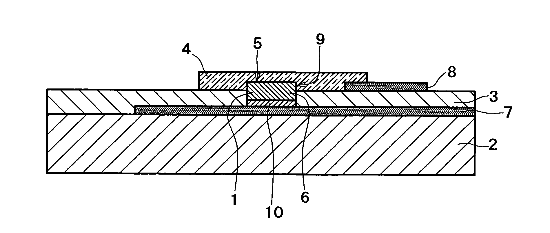
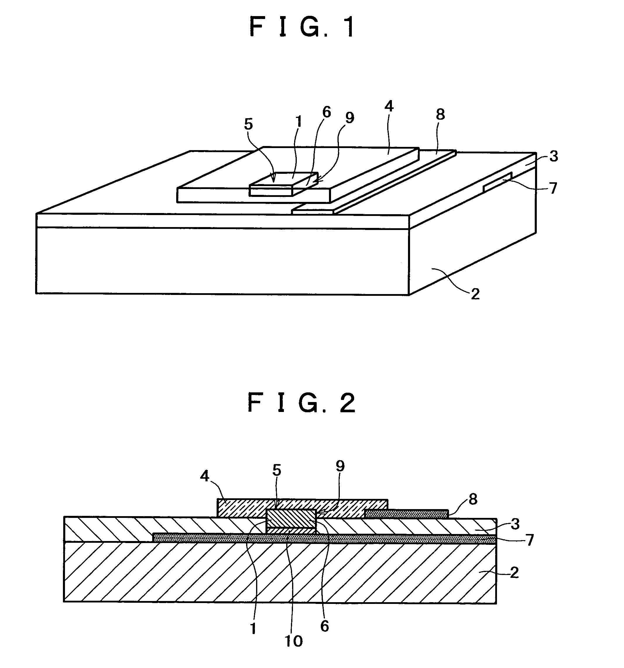
[0083]First, referring to FIGS. 1 and 2, an example of the light-emitting device according to the present invention will be described. While a light-emitting diode will be taken as an example of the light-emitting device in the description of this example, the light-emitting device according to the present invention is not limited to the light-emitting diode. FIG. 1 is a perspective view showing the condition where a light-emitting diode 1 is disposed on a substrate 2, and FIG. 2 is a sectional view showing the condition where the light-emitting diode 1 is disposed on the substrate 2.

[0084]As shown in FIGS. 1 and 2, the light-emitting diode 1 is disposed in the state of being fixed to an insulation resin layer 3 formed on the substrate 2, and a transparent electrode 4 is formed directly so as to cover a light output surface 5.

[0085]The light-emitting diode 1 is so disposed that an n-type semiconductor layer 6 made to be of the n-type conduction type by doping with an impurity is fix...

second embodiment

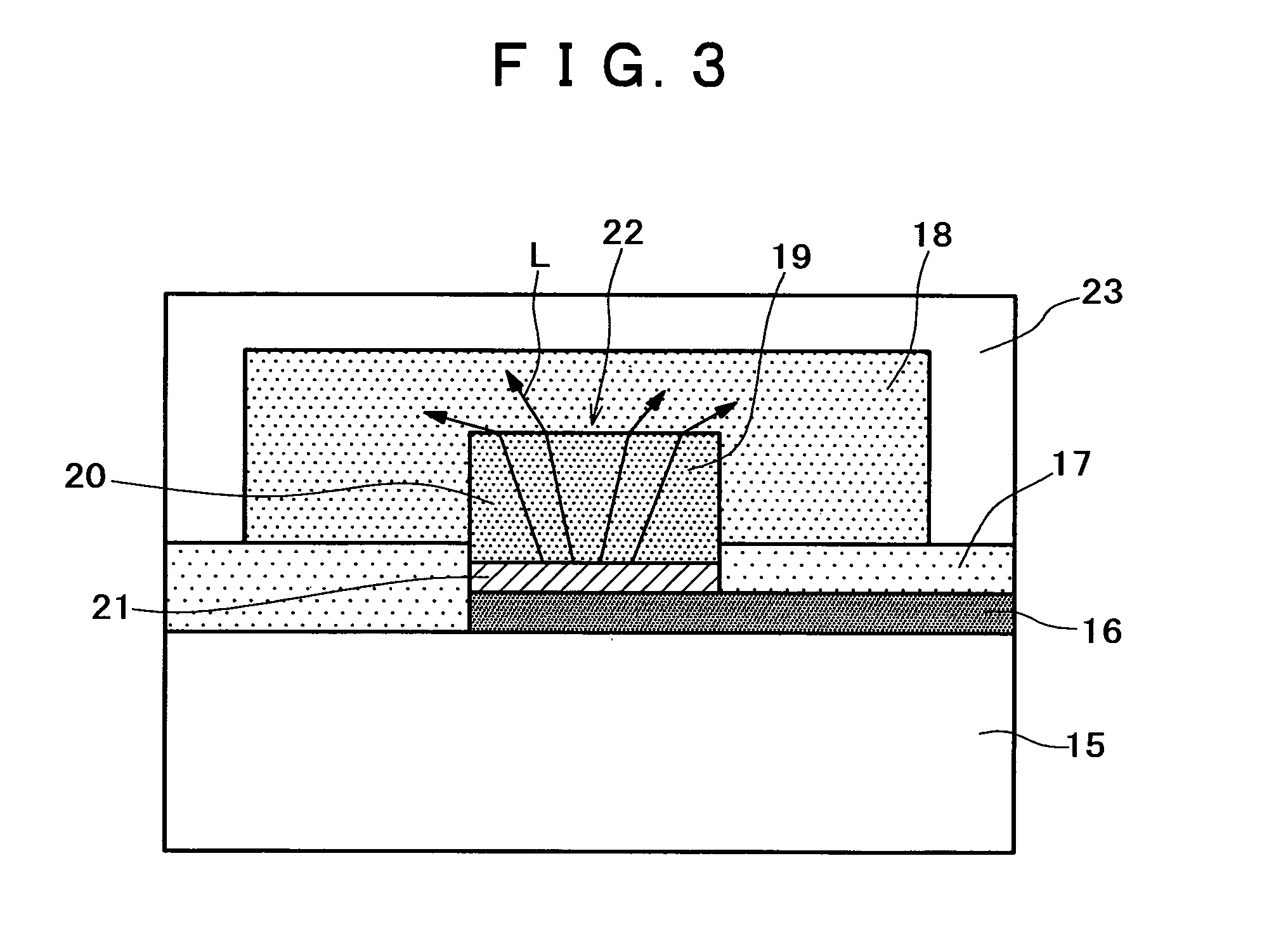
[0121]Next, as an embodiment of the present invention, an example in which electrodes are formed at parts of light output surfaces of light-emitting devices and a transparent electrode is formed so as to cover the whole areas of the light output surfaces will be described. This embodiment differs from the above-described first embodiment in that contact metals are formed on the light output surfaces of the light-emitting devices and that light emission side wiring layers are formed outside the regions of the light output surfaces. Now, a light-emitting apparatus, an image display apparatus, a method of manufacturing a light-emitting apparatus, and a method of manufacturing an image display apparatus according to the present invention will be described in detail below, referring to the drawings.

[0122]FIGS. 12A and 12B schematically illustrate the structure of a light-emitting device corresponding to one pixel in an image display apparatus formed by arranging the light-emitting device...


PUM


Abstract

Light-emitting devices, light-emitting apparatuses, image display apparatuses and methods of manufacturing same are provided. The devices and apparatuses include a transparent electrode that is connected directly to light output surfaces so as to cover the whole areas of the light output surfaces. The transparent electrode is formed to be larger in area than the light output surfaces, and are securely electrically connected to n-type semiconductor layers including the light output surfaces.

Description

CROSS REFERENCES TO RELATED APPLICATIONS[0001]This application claims priority to application of Japanese Patent Application Nos. P2003-069602 filed Mar. 14, 2003, and P2004-009777 filed Jan. 16, 2004, the disclosures of which are herein incorporated by reference.BACKGROUND OF THE INVENTION[0002]The present invention relates to a light-emitting device, a light-emitting apparatus, an image display apparatus, a method of manufacturing a light-emitting device, and a method of manufacturing an image display apparatus. More particularly, the present invention relates to a light-emitting device, a light-emitting apparatus, an image display apparatus, a method of manufacturing a light-emitting device, and a method of manufacturing an image display apparatus in which light emission efficiency is prevented from being lowered and an electrode is formed for minute light-emitting device main bodies with high accuracy.[0003]At present, in electronic apparatuses and the like, there have been wide...

Claims


Application Information

Patent Timeline
IPC IPC(8): H01L33/00G09G5/00H01L33/08H01L33/38H01L33/42
CPCH01L33/62H01L2221/68359H01L2924/0002H01L2924/00
Inventor WATANABE, TOSHIHIKODOI, MASATOSATO, NOBUAKI
Owner SONY CORP
Why Eureka
Try Eureka