
Integrated circuit with breakdown voltage multiplier

a technology of breakdown voltage multiplier and integrated circuit, which is applied in the field of integrated circuit with breakdown voltage multiplier and high-speed driver configuration, can solve the problems of limited information distribution across the communication system, limited communication hardware limitations, and severe limitations of the applicability of integrated circuits implementing such high-speed transistors

Active Publication Date: 2008-01-22
CALIFORNIA INST OF TECH
View PDF3 Cites 16 Cited by
  • Summary
  • Abstract
  • Description
  • Claims
  • Application Information

AI Technical Summary

Benefits of technology

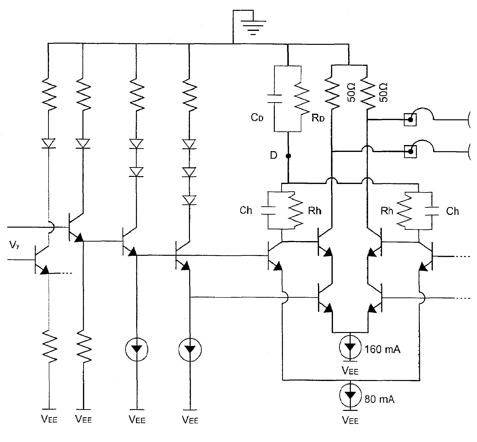
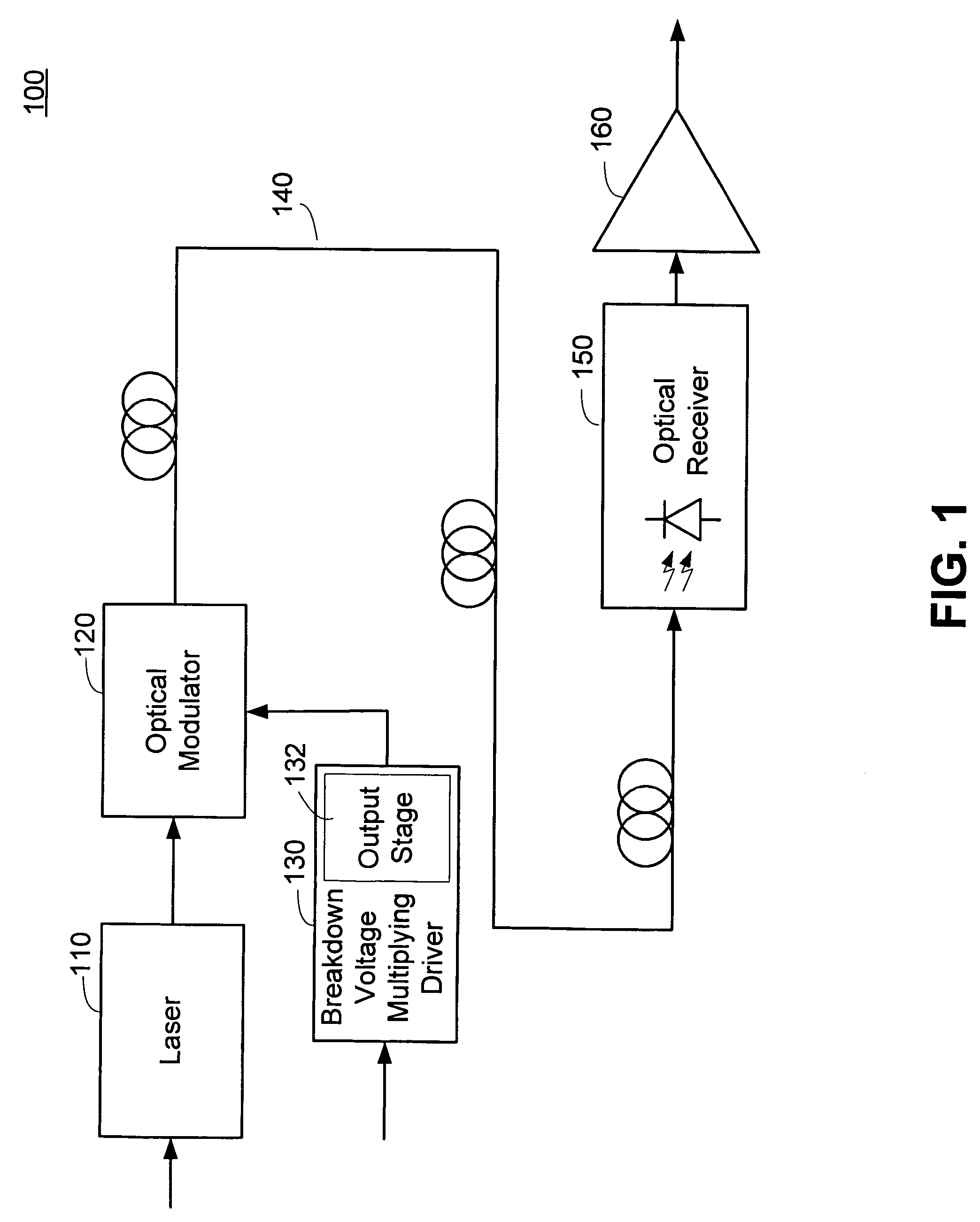
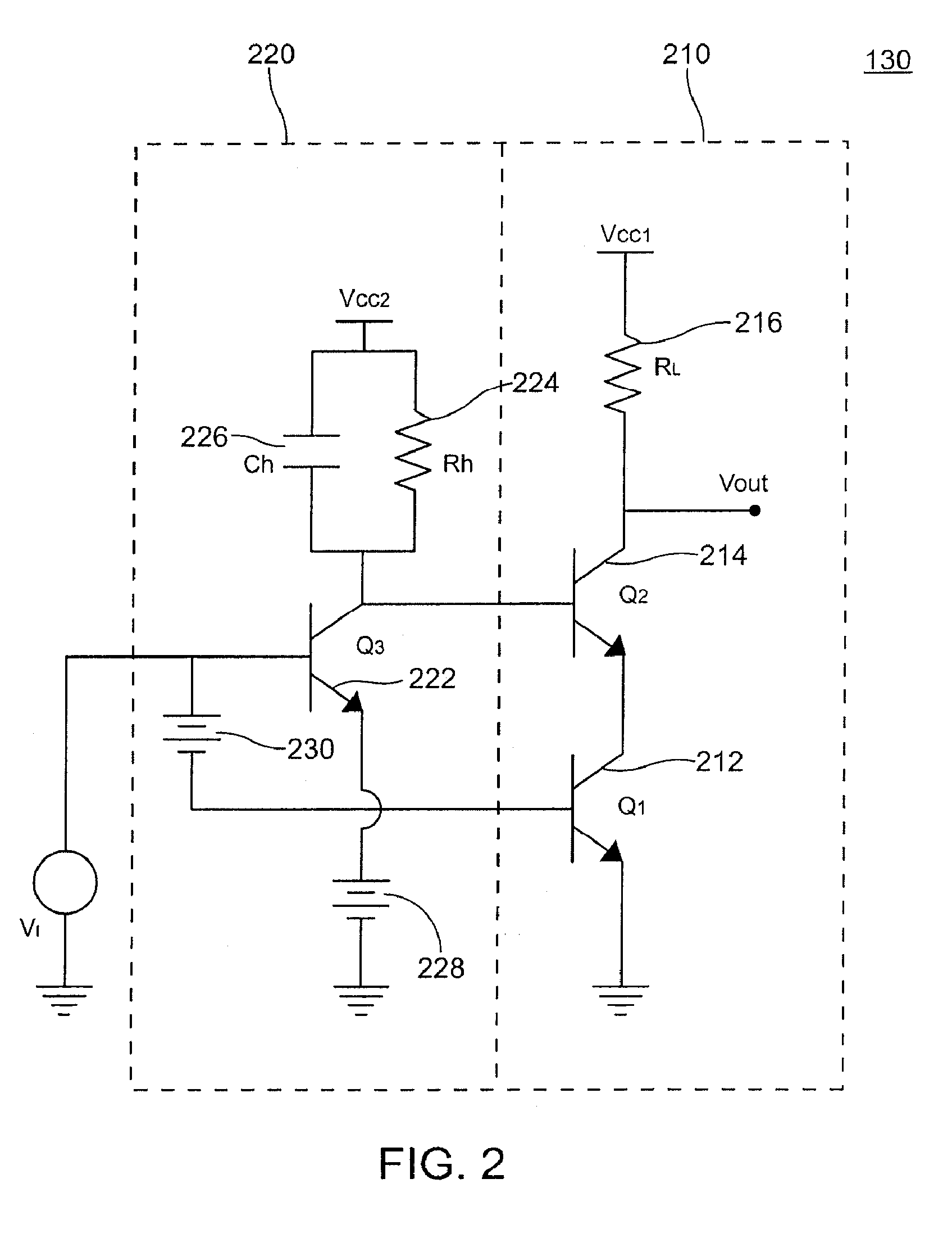
The patent describes an apparatus and method for driving an output signal in a high-speed integrated circuit. The apparatus includes a driver that can exceed the breakdown voltage of any individual element in the output driver. The driver is configured to distribute the output voltage equally among each of the transistors in the stack, allowing it to source an output voltage swing that is greater than the breakdown voltage of any individual transistor. The integrated circuit device includes a plurality of output transistors arranged in a stacked configuration, and a signal distributor configured to receive an input signal and generate a plurality of intermediate driver signals that contribute to the output signal. The output signal has a voltage swing that exceeds the breakdown voltage of any individual transistor in the driver. The method includes level shifting the input signal, generating intermediate driver signals, and coupling them to the output transistors in a stacked configuration. The technical effect of this invention is to enable a high-speed driver to exceed the breakdown voltage of any individual element in the output driver, and to distribute the output voltage equally among each of the transistors in the output stage.

Problems solved by technology

A communication system can have sufficient bandwidth allocated for distribution of vast amounts of information, but the rate that the information can be distribute across the communication system may be limited by the limitations of the communications hardware.
Although a reduction in the operating voltage can provide some benefits in the form of reduced power consumption, the combination of reduced operating voltage and reduced breakdown voltage can severely limit the applicability of integrated circuits implementing such high speed transistors.

Method used


Image

  • Integrated circuit with breakdown voltage multiplier
  • Integrated circuit with breakdown voltage multiplier
  • Integrated circuit with breakdown voltage multiplier

Examples


Embodiment Construction

[0023]A high speed integrated circuit driver utilizing a breakdown voltage multiplier configuration allows output voltage swings that exceed the breakdown voltage of any individual transistor within the driver. The breakdown voltage multiplier configuration utilizes a plurality of transistors, each configured to withstand only a portion of the entire output voltage swing. Thus, each transistor contributes some incremental value to the breakdown voltage of the driver output.

[0024]The transistors can be configured such that the each transistor in an output stage contributes a substantially equal amount to the total output signal. The aggregate signal from all of the output transistors can have a total voltage swing that exceeds the breakdown voltage of any individual transistor in the output stage. If each transistor in the output stage contributes substantially equal amount to the output signal, the output voltage swing can be a multiple of the breakdown voltage of each individual tr...


PUM


Abstract

An apparatus and method for driving an output signal in a high speed integrated circuit. The apparatus and methods enable the output voltage swing from the driver to exceed the breakdown voltage of any individual element in the output driver. A high speed driver can utilize one or more transistors in a stacked configuration, such that the breakdown voltage of the entire stacked configuration is based on the number of transistors in the stack. The driver is configured to distribute the output voltage substantially equally among each of the stacked transistors, such that the driver is able to source an output voltage swing that is greater than the breakdown voltage of any individual transistor in the driver.

Description

CROSS-REFERENCES TO RELATED APPLICATIONS[0001]This application claims the benefit of U.S. Provisional Application No. 60 / 562,661, filed Apr. 15, 2004, entitled BREAKDOWN VOLTAGE MULTIPLIER; which is hereby incorporated herein by reference in its entirety.STATEMENT AS TO RIGHTS TO INVENTIONS MADE UNDER FEDERALLY SPONSORED RESEARCH OR DEVELOPMENT[0002]This invention was made with government support under grant N00014-01-1-0764 awarded by the Office of Naval Research. The government has certain rights in the invention.BACKGROUND OF THE DISCLOSURE[0003]The disclosure relates the field of electronic devices. More particularly, the disclosure relates to a high speed driver configuration that allows an output voltage swing to exceed the breakdown voltage of any individual transistor in the driver.[0004]Processors and associated applications have developed to a level that enable enormous amounts of information to be generated and utilized. The capability of processors and associated applica...

Claims


Application Information

Patent Timeline
Patent Type & Authority Patents(United States)
IPC IPC(8): H03K19/082H03K19/003H03K19/0175
CPCH03K19/00307H03K19/00315
Inventor MANDEGARAN, SAMHAJIMIRI, SEYED ALI
Owner CALIFORNIA INST OF TECH
Learn More