Apparatus for treating substrate

a technology of apparatus and substrate, applied in the direction of electrical apparatus, decorative surface effects, decorative arts, etc., can solve the problems of long work time and large amount of etchant consumption, and achieve the effect of preventing a yield drop and high speed

Active Publication Date: 2008-01-29
SEMES CO LTD
View PDF30 Cites 28 Cited by
  • Summary
  • Abstract
  • Description
  • Claims
  • Application Information

AI Technical Summary

Benefits of technology

[0004]Exemplary embodiments of the present invention are directed to apparatus and method for treating a substrate to etch the top edge and the bottom of the substrate at a high speed and to prevent a yield lowering caused by an isotropic etch that is a wet etch. In an exemplary embodiment, the apparatus includes a substrate support part, a wet etch part, and a dry etch part. The substrate support part has a rotatable support plate and a support pin protruding from a top surface of the support plate to support a substrate to be spaced apart from a top surface of the support plate. The wet etch part supplies an etchant to a space between a substrate placed on the support pin and the support plate to perform an etch, and a dry etch part supplies plasma to the top edge of a substrate placed on the support plate to perform an etch.

Problems solved by technology

Further, the above-described method includes protecting a pattern-formed portion with a protectant or a mask and re-removing the same, which results in a long work time and consumption of a large amount of etchant.

Method used


Image

  • Apparatus for treating substrate
  • Apparatus for treating substrate
  • Apparatus for treating substrate

Examples


Embodiment Construction

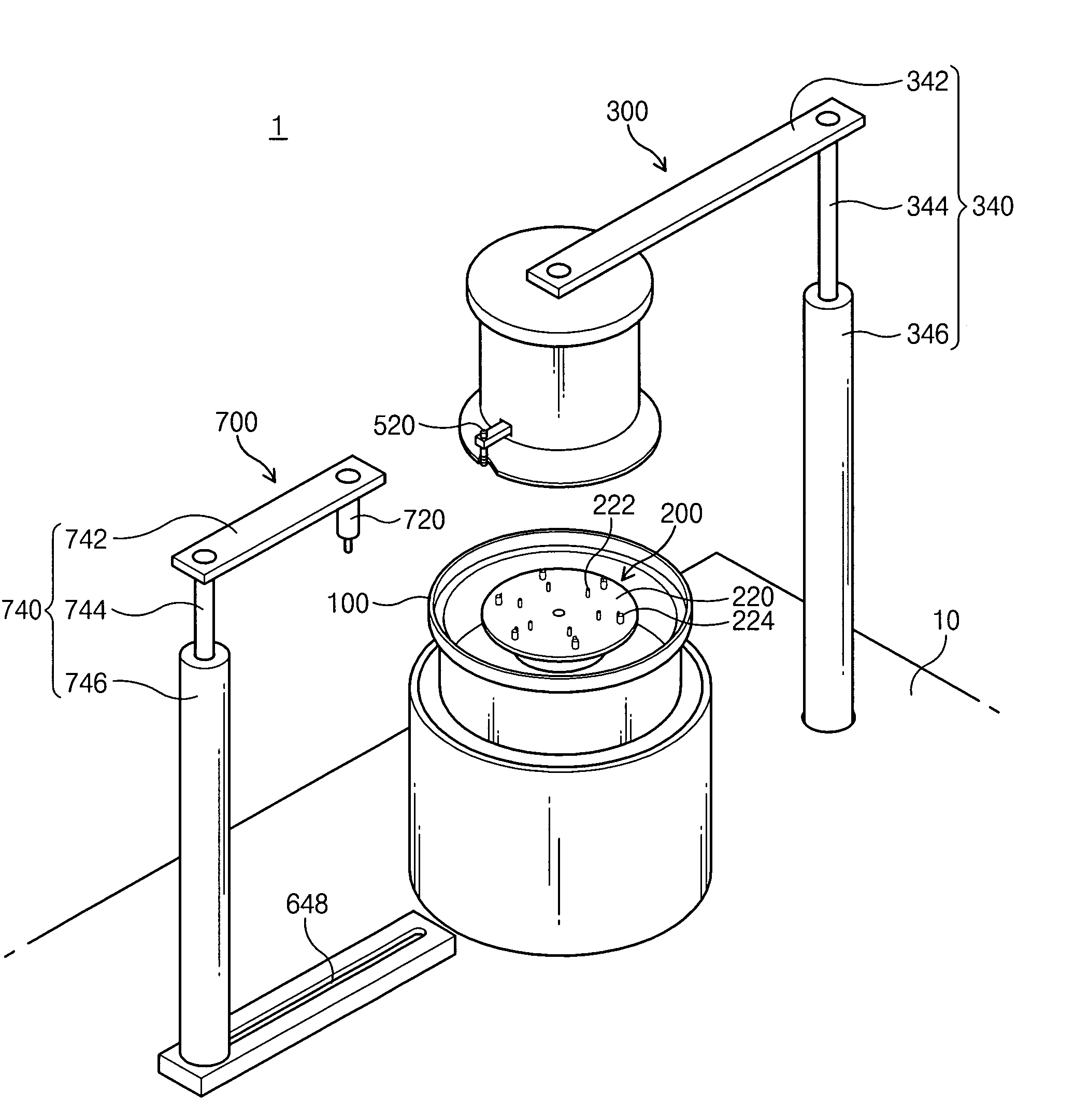
[0033]The present invention will now be described more fully hereinafter with reference to the accompanying drawings, in which a preferred embodiment of the invention is shown. The invention may, however, be embodied in different forms and should not be construed as limited to the embodiments set forth herein. Rather, these embodiments are provided so that this disclosure will be thorough and complete, and will fully convey the scope of the invention to those skilled in the art. In the drawings, the height of layers and regions are exaggerated for clarity.

[0034]In the embodiment of the invention, a top surface (24 of FIG. 8) of a wafer (20 of FIG. 8) means a pattern-formed one of both surfaces of the wafer, and a bottom surface (22 of FIG. 8) thereof means the other surface. Hereinafter, a to-be-etched portion of the top surface will be referred to as “edge” and a to-be-unetched portion thereof will be referred to as “non-etch portion” (24b of FIG. 8)”.

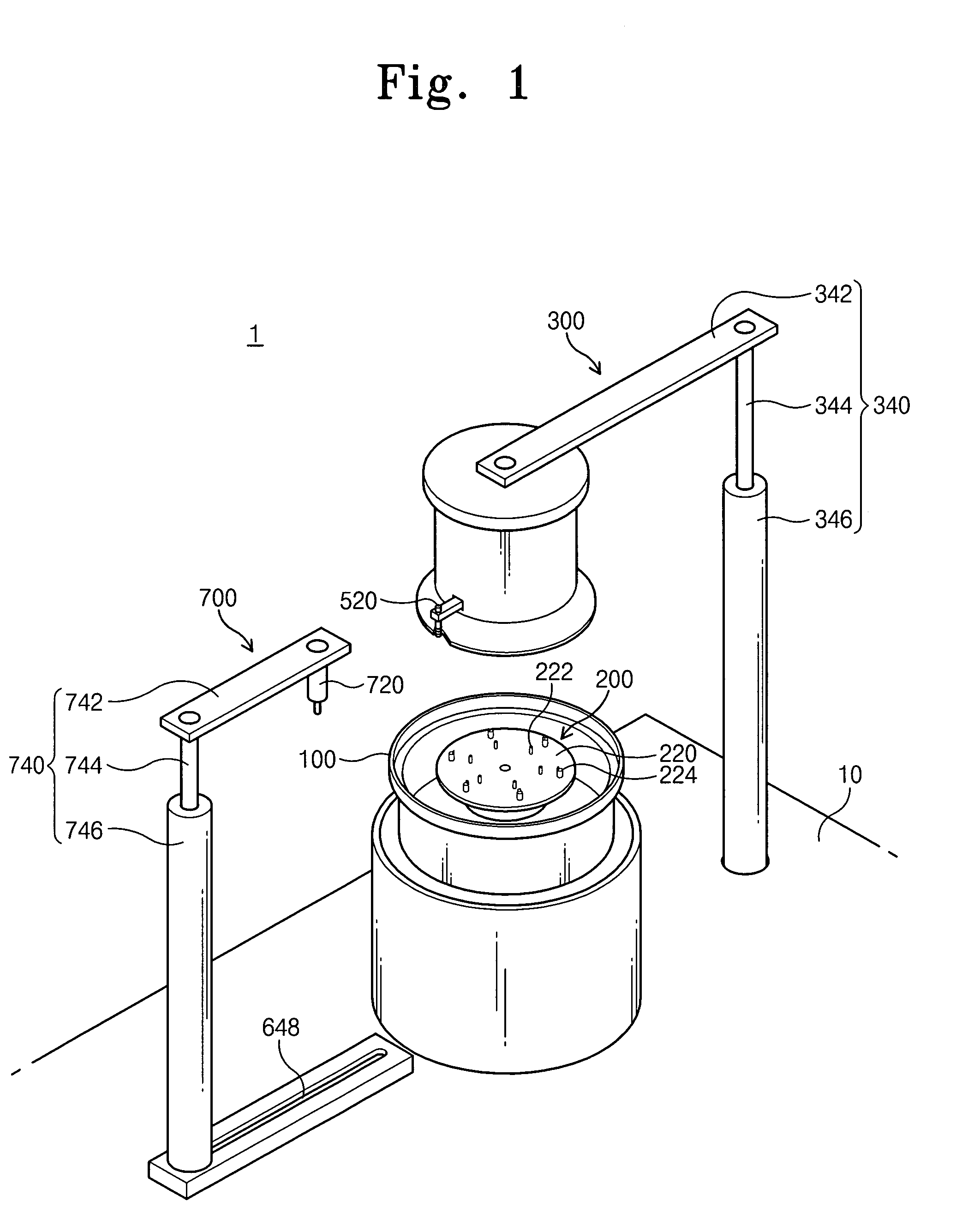
[0035]FIG. 1 is a perspective ...


PUM

PropertyMeasurementUnit
chemical flowaaaaaaaaaa
dielectricaaaaaaaaaa
magnetic fieldaaaaaaaaaa

Abstract

The present is directed to an apparatus for etching the top edge and bottom of a wafer. The apparatus includes a substrate support part for supporting a wafer and a movable protect part for preventing fluid for an etch from flowing into a non-etch portion of the wafer. The top edge and bottom of the wafer is etched by a wet etch, and a boundary of the non-etch portion and the edge of the wafer is etched by a dry etch.

Description

FIELD OF THE INVENTION[0001]The present invention relates to apparatus and method for treating a substrate and, more particularly, to apparatus and method for etching the top edge and the bottom of a substrate.BACKGROUND OF THE INVENTION[0002]A plurality of layers such as polysilicon, oxide, nitride, and metal are deposited on a wafer that is used as a semiconductor substrate in a semiconductor fabricating process. A photoresist layer is coated on the layer. A pattern drawn on a photo mask using an exposure process is transcribed to the photoresist layer. An etching process is carried out to form a desired pattern on the wafer. Foreign substances such as various layers or photoresist remain the top edge or the bottom of a wafer where the above-mentioned processes are carried out. If the edge of a held wafer is transferred, the foreign substances are separated from the wafer to be dispersed. The dispersed substances contaminate an apparatus and act as particles in subsequent processe...

Claims


Application Information

Patent Timeline
Patent Type & Authority Patents(United States)
IPC IPC(8): C23F1/00H01L21/00H01L21/304H01L21/3065H01L21/306
CPCH01L21/67051H01L21/67086H01L21/67069
Inventor KIM, IN-JUNCHO, JUNG-KEUNCHOI, JANG-SEOBCHOI, YONG-NAMBAE, JEONG-YONG
Owner SEMES CO LTD
Why Eureka
Try Eureka