Plasma display panel having high brightness and high contrast using light absorption reflection film

a technology of light absorption reflection film and display panel, which is applied in the direction of gas-filled discharge tubes, optical/shielding arrangements, electric discharge tubes, etc., can solve the problems of reduced contrast, increased difficulty in detecting the presence of light, and reduced brightness, so as to achieve efficient reflected visible light emitted

Inactive Publication Date: 2008-01-29
SAMSUNG SDI CO LTD
View PDF34 Cites 154 Cited by
  • Summary
  • Abstract
  • Description
  • Claims
  • Application Information

AI Technical Summary

Benefits of technology

[0012]The present invention provides a plasma display panel having a light absorption reflection film that does not reflect external light infiltrated into the plasma display panel and efficiently reflects visible light emitted from a discharge space.

Problems solved by technology

However, because the bus electrodes are not arranged in the non-discharge region of the plasma display panel, contrast is reduced due to reflection of external light infiltrated into the plasma display panel through a non-discharge region.
However, brightness is reduced since the light absorption reflection film absorbs visible light emitted from the discharge space because it is black.
This problem becomes more severe as the width of the light absorption reflection film is increased to further increase the contrast.

Method used


Image

  • Plasma display panel having high brightness and high contrast using light absorption reflection film
  • Plasma display panel having high brightness and high contrast using light absorption reflection film
  • Plasma display panel having high brightness and high contrast using light absorption reflection film

Examples


first embodiment

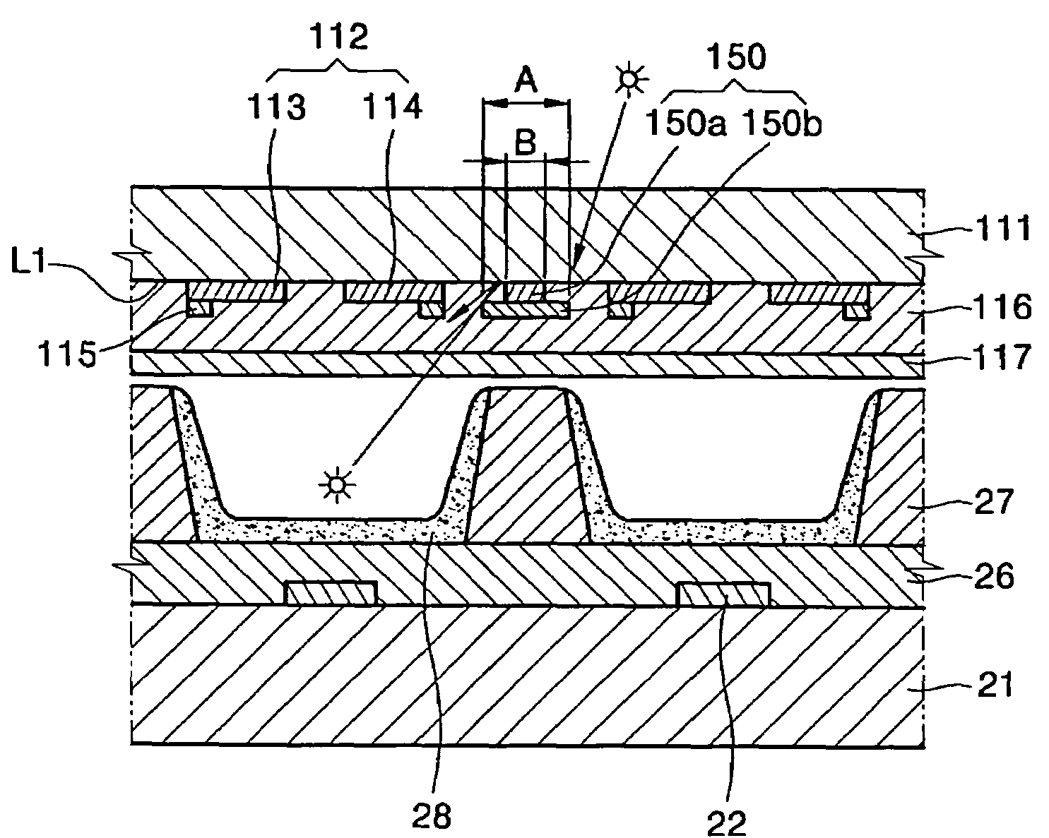
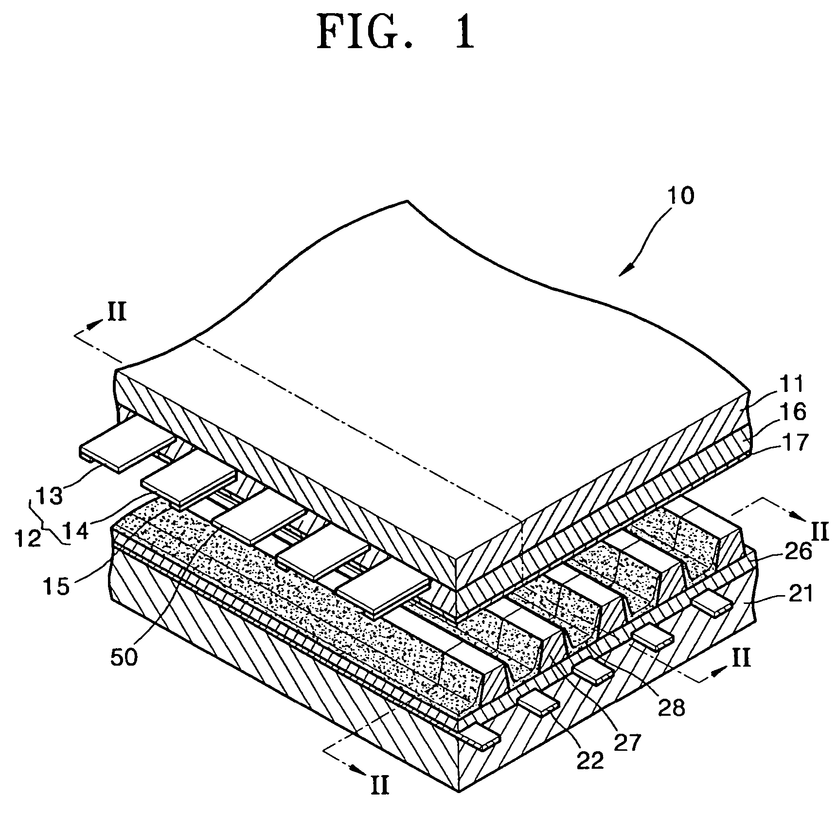
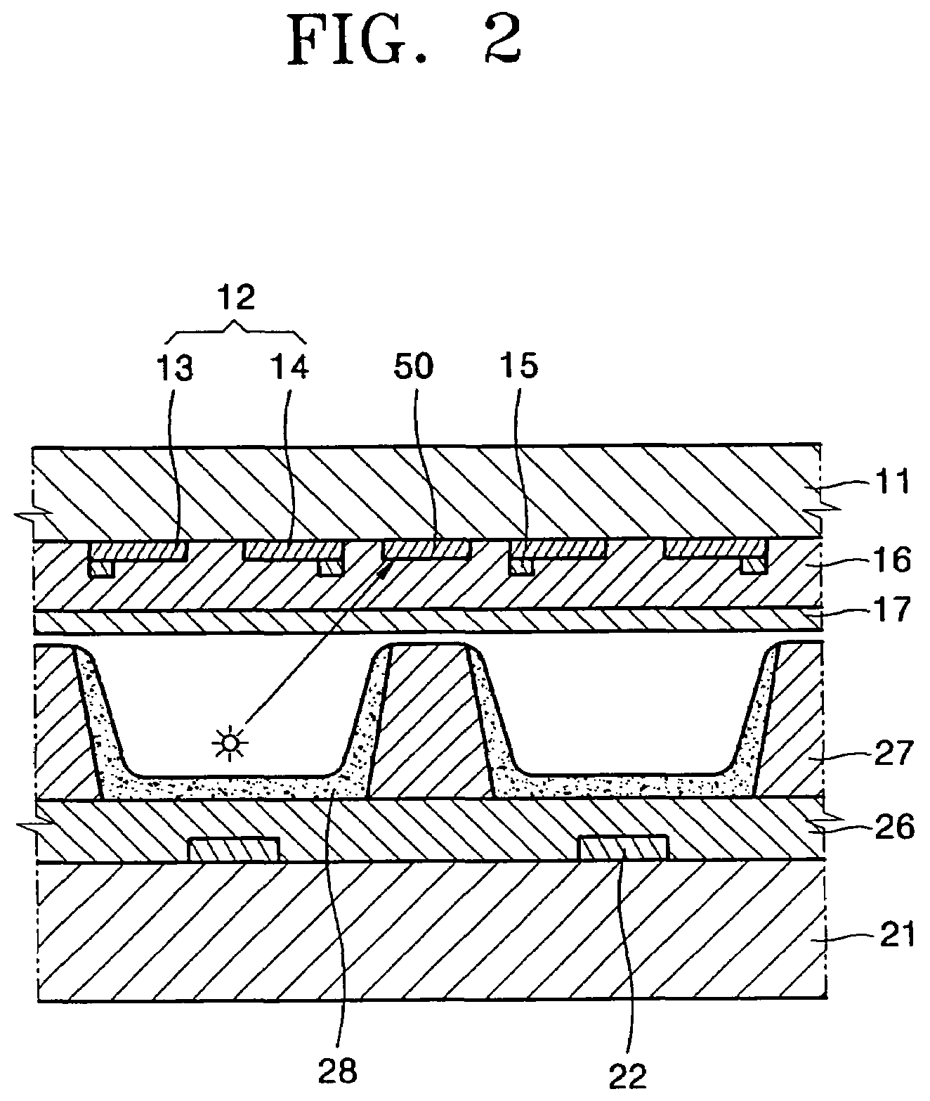
[0063]Referring to FIG. 3, a plasma display panel 100 according to the present invention comprises a front substrate 111, sustain electrode pairs 112 composed of X electrodes 113 and Y electrodes 114, a front dielectric layer 116, a rear substrate 21, address electrodes 22, a rear dielectric layer 26, barrier ribs 27, and a fluorescent material 28.

[0064]The plasma display panel 100 according to the present invention can include a protective layer 117.

[0065]Address electrodes 22 that generate an address discharge and have a predetermined pattern, such as a stripe pattern, are disposed on a side surface of the rear substrate 21. The address electrodes 22 are covered by the rear dielectric layer 26. Barrier ribs 27 that define discharge cells and prevent cross-talk of charged electrons between cells are disposed on the rear dielectric layer 26. The barrier ribs 27 can be arranged parallel to the address electrodes 22 or can be arranged by forming second barrier ribs (not shown) to cros...

second embodiment

[0076]FIG. 8 is a perspective view of a plasma display panel 200 according to the present invention. A rear substrate 21, address electrodes 22, a rear dielectric layer 26, barrier ribs 27, and fluorescent material 28 are not depicted since their structures and functions are the same as in FIG. 3, and a detailed description of these parts has also been omitted.

[0077]Referring to FIG. 8, the plasma display panel 200 comprises a front substrate 211, sustain electrode pairs 212 composed of X electrodes 213 and Y the electrodes 214, and a front dielectric layer 216. A protective layer 217 is provided. However, the present invention is not limited thereto and the present invention also includes a plasma display panel 200 without a protective layer. Bus electrodes 215 are arranged on a lower surface of the sustain electrode pairs 212 but the bus electrodes 215 can be omitted or the sustain electrode pairs 212 can be formed of only bus electrodes 215.

[0078]A light absorption reflection fil...

third embodiment

[0088]FIG. 9 is a perspective view of a plasma display panel 300 according to the present invention. The rear substrate 21, the address electrodes 22, the rear dielectric layer 26, the barrier ribs 27, and the fluorescent material 28 are not shown since the structures and functions are identical to the plasma display panel 100 depicted in FIG. 3, and a detailed description thereof has been omitted.

[0089]Referring to FIG. 9, the plasma display panel 300 comprises a front substrate 311, sustain electrode pairs 312 composed of X electrodes 313 and Y the electrodes 314, and a front dielectric layer 316. Bus electrodes 315 are arranged on a lower surface of the sustain electrode pairs 312. However, the bus electrodes 315 can be omitted or the sustain electrode pairs 312 can be formed of only bus electrodes 315.

[0090]A light absorption reflection film 350 is arranged on a lower surface of the front dielectric layer 316. In FIG. 9, the light absorption reflection film 350 is arranged on th...


PUM


Abstract

A plasma display panel having a light absorption reflection film that does not reflect light emitted from a discharge space in a non-discharge region includes: a rear substrate; a plurality of address electrodes arranged on a surface of the rear substrate; a rear dielectric layer arranged on the rear substrate to cover the address electrodes; a plurality of barrier ribs arranged on the rear dielectric layer to define discharge cells; a front substrate facing the rear substrate; a plurality of sustaining electrode pairs composed of X and Y electrodes; a light absorption reflection film including a first light absorption reflection film arranged between the adjacent sustaining electrode pairs and a second light absorption reflection film having a different width than that of the first light absorption reflection film, the second light absorption reflection film arranged on a lower surface of the first light absorption reflection film; and a front dielectric layer arranged on a lower surface of the front substrate to cover the X and Y electrodes and the light absorption reflection film.

Description

CLAIM OF PRIORITY[0001]This application makes reference to, incorporates the same herein, and claims all benefits accruing under 35 U.S.C. § 119 from an application for PLASMA DISPLAY PANEL HAVING HIGH BRIGHTNESS AND HIGH CONTRAST earlier filed in the Korean Intellectual Property Office on 21 Oct. 2003 and there duly assigned Serial No. 2003-73423.BACKGROUND OF THE INVENTION[0002]1. Field of the Invention[0003]The present invention relates to a plasma display panel, and more particularly, to a plasma display panel having a front substrate with a structure to improve brightness and maintain a high contrast.[0004]2. Description of the Related Art[0005]A plasma display panel, generally considered to be a display device that will replace conventional cathode ray tubes, obtains an image by exciting a fluorescent material arranged in a predetermined pattern with ultraviolet rays generated by a discharge gas sealed in a space formed by two substrates on which a plurality of electrodes are ...

Claims


Application Information

Patent Timeline
Patent Type & Authority Patents(United States)
IPC IPC(8): H01J17/49
CPCH01J11/12H01J11/44H01J2211/444
Inventor HONG, CHONG-GIKANG, TAE-KYOUNG
Owner SAMSUNG SDI CO LTD
Why Eureka
Try Eureka