Staggered memory cell array

a memory cell array and staggered technology, applied in the field of electromechanical circuits, can solve the problems of limited state-of-the-art fabrication equipment, limited geometric feature size and space reduction of semiconductor integrated circuits, and significant challenges for manufacturers of portable electronic devices, so as to reduce the size of arrays, reduce cell size, and increase critical distances

Active Publication Date: 2008-02-05
TEXAS INSTR INC
View PDF3 Cites 110 Cited by
  • Summary
  • Abstract
  • Description
  • Claims
  • Application Information

AI Technical Summary

Benefits of technology

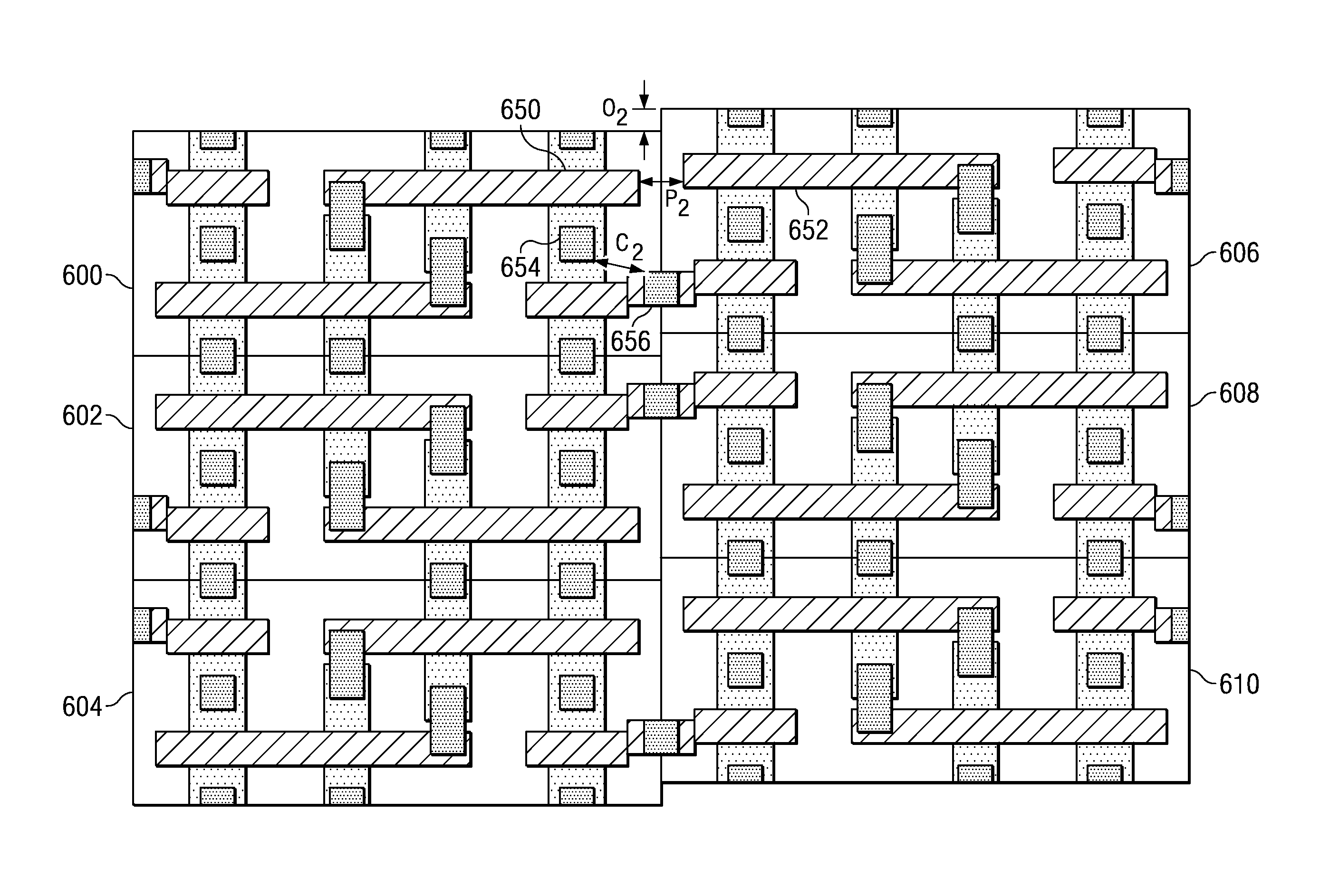
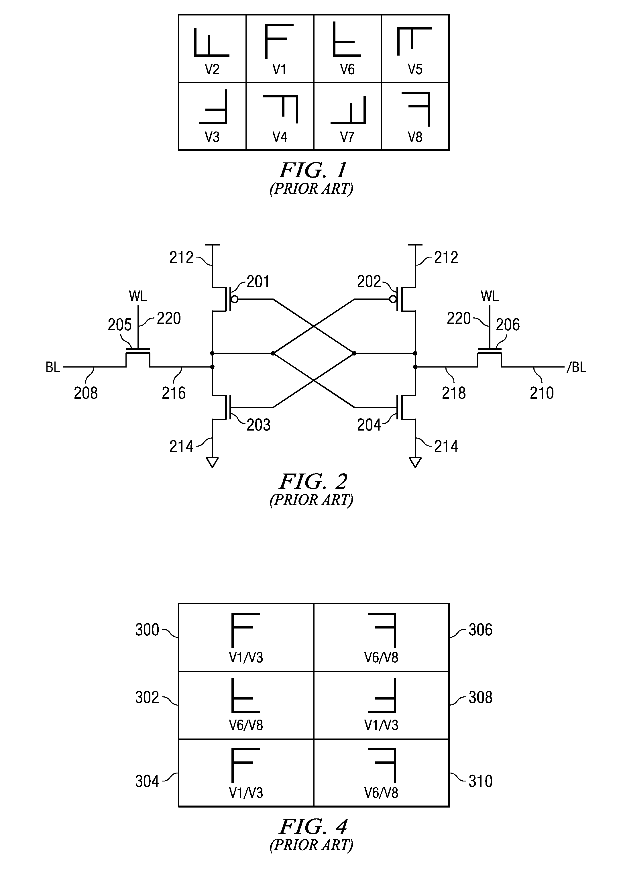
[0008]In accordance with a preferred embodiment of the invention, there is disclosed a method of placing a cell in an array. The cell is placed a plurality of times in a first array in alternating views. The cell is also placed a plurality of times in a second array in alternating views. The second array is placed adjacent and offset from the first array by an offset distance. The offset increases critical distances between adjacent cells and permits a corresponding reduction of cell size. Array size is reduced without degrading yield.

Problems solved by technology

The continuing popularity of portable electronic devices presents manufacturers with significant challenges.
Geometric feature size and space reduction of semiconductor integrated circuits, however, is limited by state-of-the-art fabrication equipment.
Reduction of geometric feature sizes and spaces beyond manufacturing equipment capability inevitably results in short or open circuit conditions of the multi-layer geometric features.
These short or open circuit conditions often render the semiconductor integrated circuit inoperable, thereby degrading yield, the functional fraction of total semiconductor integrated circuit product.
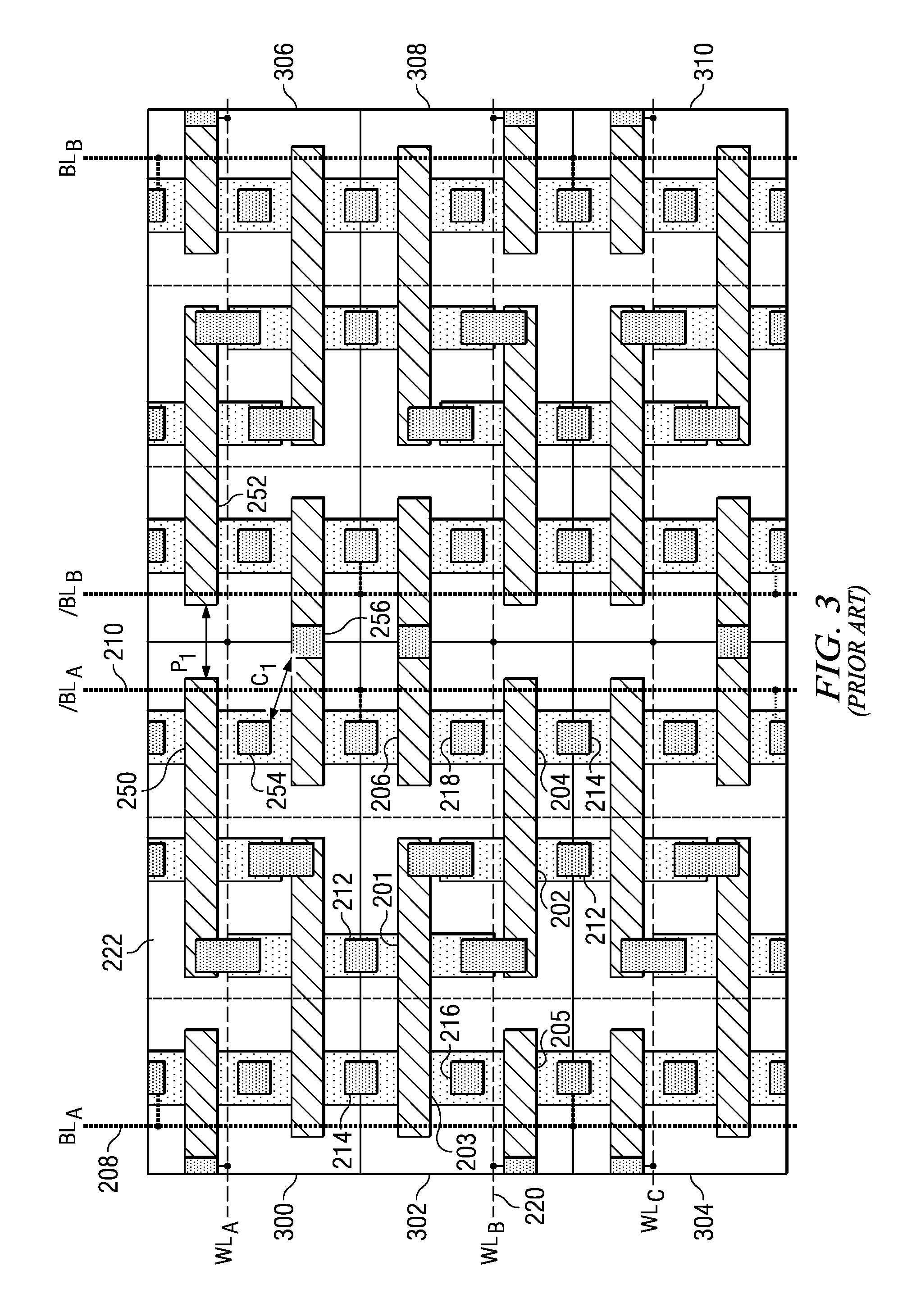
In general, any of these design rules may limit the horizontal or vertical dimensions of the memory cell.
As such, these limiting design rules are critical dimensions and may not be further reduced without increasing the probability of shorting.
Because they are aligned end-to-end they cannot be moved closer together without increased shorting of the polycrystalline silicon geometries and decreased yield.
Thus, the individual memory cell size and corresponding array size are limited by these critical dimensions.

Method used


Image

  • Staggered memory cell array
  • Staggered memory cell array
  • Staggered memory cell array

Examples


Embodiment Construction

[0030]Referring to FIG. 17, there is a block diagram of a wireless telephone as an example of a portable electronic device which could advantageously employ this invention in memory arrays, decode circuits, interconnect cells, or any other geometrical array as is known in the art. The wireless telephone includes antenna 1700, radio frequency transceiver 1702, baseband circuits 1710, microphone 1706, speaker 1708, keypad 1720, and display 1722. The wireless telephone is preferably powered by a rechargeable battery (not shown) as is well known in the art. Antenna 1700 permits the wireless telephone to interact with the radio frequency environment for wireless telephony in a manner known in the art. Radio frequency transceiver 1702 both transmits and receives radio frequency signals via antenna 1702. The transmitted signals are modulated by the voice / data output signals received from baseband circuits 1710. The received signals are demodulated and supplied to baseband circuits 1710 as ...


PUM


Abstract

A method of placing a cell in an array is disclosed. The method includes placing the cell a plurality of times (600, 602, 604) in a first array. The cell is also placed a plurality of times (606, 608, 610) in a second array. The second array is placed adjacent and offset from the first array by an offset distance (O2).

Description

FIELD OF THE INVENTION[0001]This invention generally relates to electronic circuits, and more specifically to geometric layout efficiency of semiconductor integrated circuits.BACKGROUND OF THE INVENTION[0002]The continuing popularity of portable electronic devices presents manufacturers with significant challenges. Increasing capability of electronic devices is moderated by considerations of cost, size, weight, and battery life. These considerations have increasingly resulted in higher levels of semiconductor integration. Thus, portable electronic devices frequently embed memory, control, signal processors, and other circuit functions on a single integrated circuit. Further optimization of these portable electronic devices dictates even greater reduction in geometric feature sizes and spaces between these geometric features. Geometric feature size and space reduction of semiconductor integrated circuits, however, is limited by state-of-the-art fabrication equipment. Reduction of geo...

Claims


Application Information

Patent Timeline
Patent Type & Authority Patents(United States)
IPC IPC(8): G11C5/06H01L27/11
CPCH01L27/1104H10B10/12G11C5/06G11C7/10
Inventor SADRA, KAYVANHOUSTON, THEODORE W.
Owner TEXAS INSTR INC
Why Eureka
Try Eureka