Electromagnetic radiation absorber based on magnetic microwires

a technology of electromagnetic radiation absorber and magnetic microwire, which is applied in the direction of radio wave reradiation/reflection, measurement devices, instruments, etc., can solve the problems of increasing electromagnetic interference, radar interference, and reducing performan

Active Publication Date: 2008-02-26
MICROMAG 2000
View PDF8 Cites 11 Cited by
  • Summary
  • Abstract
  • Description
  • Claims
  • Application Information

AI Technical Summary

Benefits of technology

[0041]For a given microwire density, control of the thickness e2 of the intermediate region in which the microwires are embedded allows increasing or decreasing the central frequency absorption level at the expense of decreasing or increasing the bandwidth, respectively.
[0042]The absorption level can be controlled by increasing the thickness e1 of the dielectric region between the exterior and the microwires.
[0043]The increase in thickness e1 allows greater stability of the standing wave inside the absorbent sheet.
[0044]The total thickness e of the absorbent sheet can be decreased by increasing its dielectric constant.

Problems solved by technology

The large number of electronic systems built into vehicles gives rise to an increase in electromagnetic interferences.
This problem includes false images, radar interferences and a decrease in performance due to the coupling between various systems.
This method has little practical use since the absorber is too thick and is effective only for excessively narrow frequency bands and variations of angles of incidence.
The usefulness of the method is limited due to the large thickness of the dielectric sheet and the narrow absorption band they have, particularly at low frequencies.
However, when metallic particles are dispersed, high permeabilities in the order of 10 or 100 are not compatible with low conductivities in the order of 10−2 or 10−8 mohm per meter.

Method used


Image

  • Electromagnetic radiation absorber based on magnetic microwires
  • Electromagnetic radiation absorber based on magnetic microwires
  • Electromagnetic radiation absorber based on magnetic microwires

Examples


Embodiment Construction

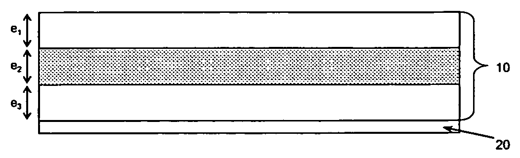
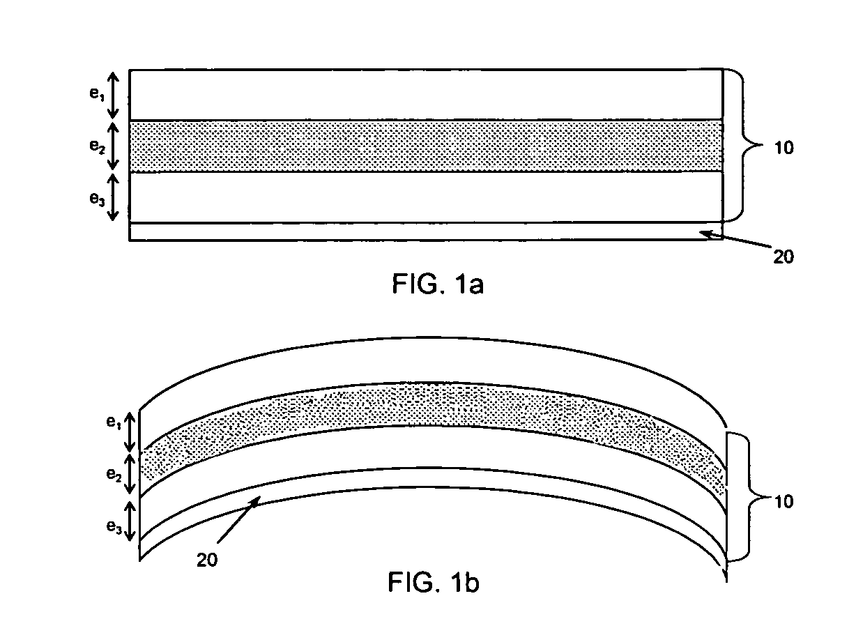
[0058]FIG. 1a shows a diagram of an absorber, in this case, an absorption plate in which the absorbent sheet 10 (or dielectric support) and metallic sheet 20 are distinguished.

[0059]The absorbent sheet is characterized by a given dielectric constant and has thickness e, which is divided into three regions of thicknesses e1, e2 and e3, respectively. The intermediate region of thickness e2 contains the microwires in the suitable percentage and with optimal magnetic and geometric (diameter and length) properties. Optimization of the absorption properties of the sheet is conditioned to the adjustment of said thicknesses. Said thicknesses are in turn conditioned by the dielectric constant of each and every one of the sheets.

[0060]FIG. 1b shows a similar diagram to that of FIG. 1a, but for another type of geometry.

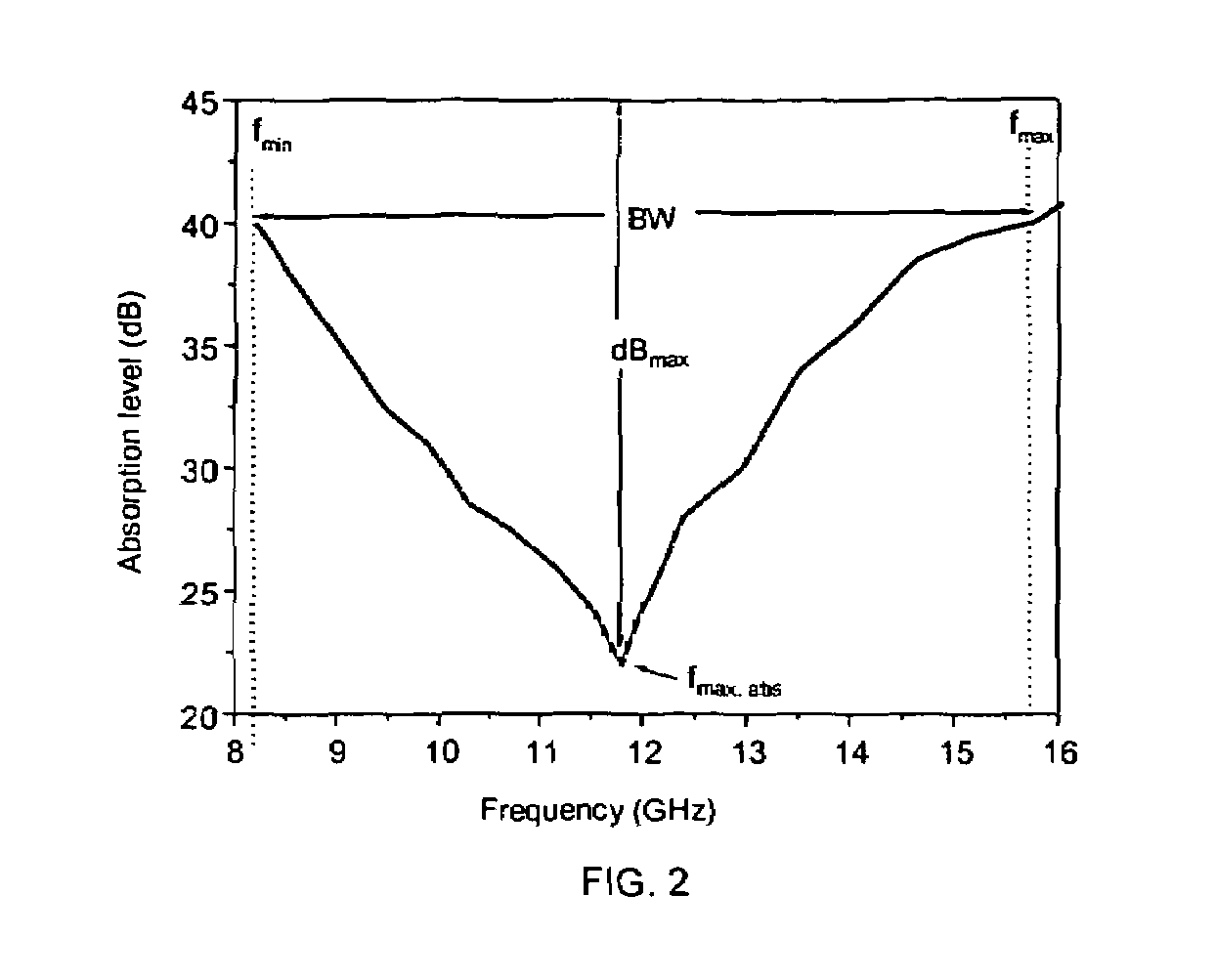
[0061]The absorption spectrum associated to each absorber is characterized by three fundamental parameters: frequency associated to the maximum absorption peak fmax abs., bandwi...


PUM


Abstract

The invention relates to an electromagnetic radiation absorber for a preselected frequency range, comprising:an absorbent sheet (10) located such that said electromagnetic radiation falls on it, anda conductive base (20) located under said absorbent sheet, wherein said absorbent sheet:has a total thickness e exceeding λ / (ε)1 / 24, where λ is the wavelength of the incident electromagnetic radiation, andis made up of a dielectric material containing amorphous magnetic microwires, the magnetic permeability of which in the preselected frequency range has an imaginary part μ″ which is at least 100 times greater than the corresponding real part μ′, said microwires being distributed in a volume having a thickness e2 of at least λ / (ε)1 / 216, where ε is the dielectric constant of the absorbent sheet and said volume is located a distance e3 from the conductive base that is not less than λ / (ε)1 / 28.

Description

BACKGROUND OF THE INVENTION[0001](1) Field of the Invention[0002]The present invention refers to an electromagnetic radiation absorber based on magnetic microwires.[0003]The invention is encompassed within the technical field of magnetic materials, also covering aspects of electromagnetism, applicable in the field of magnetic sensors and absorbers and the field of metallurgy.[0004](2) Description of Related Art[0005]Numerous applications require eliminating reflections from electromagnetic radiation. The large number of electronic systems built into vehicles gives rise to an increase in electromagnetic interferences. This problem includes false images, radar interferences and a decrease in performance due to the coupling between various systems. A microwave absorber might be very effective for eliminating this type of problems. There is even greater interest in reducing the radar cross section of certain systems to prevent or minimize their detection.[0006]Microwave absorbers are ca...

Claims


Application Information

Patent Timeline
Patent Type & Authority Patents(United States)
IPC IPC(8): H01Q17/00G01S13/00
CPCH01Q17/002H01Q17/007
Inventor MARIN PALACIOS, PILARHERNANDO GRANDE, ANTONIOCORTINA BLANCO, DANIELGOMEZ REBOLLEDO, JOSE JUANCALVO ROBLEDO, JAVIER
Owner MICROMAG 2000
Why Eureka
Try Eureka