Switching power source apparatus with voltage gate detector for the switch

a technology of voltage gate detector and switch, which is applied in the direction of pulse technique, process and machine control, instruments, etc., can solve the problems of increasing the cost of the difficulty of fabricating the switching power source apparatus into a small-size package, etc., and achieve the effect of preventing an erroneous operation of the switching element and increasing the impedan

Active Publication Date: 2008-02-26
SANKEN ELECTRIC CO LTD
View PDF9 Cites 7 Cited by
  • Summary
  • Abstract
  • Description
  • Claims
  • Application Information

AI Technical Summary

Benefits of technology

[0006]A switching power source apparatus employing the quasi-resonance control method is generally manufactured by integrating a part of the apparatus into a semiconductor integrated circuit and by fabricating the apparatus into a small-size package, to improve mass productivity.
[0007]The switching power source apparatus according to the related art should design and prepare dedicated terminals on a semiconductor integrated circuit on which the primary circuit and controller are integrated, to directly connect the semiconductor integrated circuit to the tertiary winding of the transformer. This configuration makes it difficult to fabricate the switching power source apparatus into a small-size package. To detect a voltage generated on the tertiary winding of the transformer, the tertiary winding must be connected to rectification elements such as diodes. This increases the cost of the switching power source apparatus. There is a need, therefore, for a circuit configuration applicable for a switching power source apparatus, capable of achieving the quasi-resonance control method to reduce a switching loss and noise without forming dedicated terminals on a semiconductor integrated circuit for connecting the semiconductor integrated circuit to a tertiary winding of a transformer.
[0008]According to the present invention, a switching power source apparatus capable of reducing package size and cost, realizing the quasi-resonance control method to reduce a switching loss and noise, and simplifying the structure of the apparatus can be provided.
[0013]According to a fifth aspect based on the first aspect of the present invention, the driver includes a first drive element configured to output a high-level voltage to the gate of the switching element in response to the ON control signal from the controller, a second drive element configured to output a ground-level voltage, and an OFF command circuit configured to prevent an erroneous operation of the switching element. The OFF command circuit temporarily turns off the second drive element after the switching element is turned off from an ON state, to increase impedance between the gate of the switching element and the ground. At the same time, the OFF command circuit clamps, directly or indirectly through the second drive element, an amplitude voltage of free oscillation occurring at the gate of the switching element so that the amplitude voltage of free oscillation may not exceed a predetermined level.

Problems solved by technology

This configuration makes it difficult to fabricate the switching power source apparatus into a small-size package.
This increases the cost of the switching power source apparatus.

Method used


Image

  • Switching power source apparatus with voltage gate detector for the switch
  • Switching power source apparatus with voltage gate detector for the switch
  • Switching power source apparatus with voltage gate detector for the switch

Examples


first modification

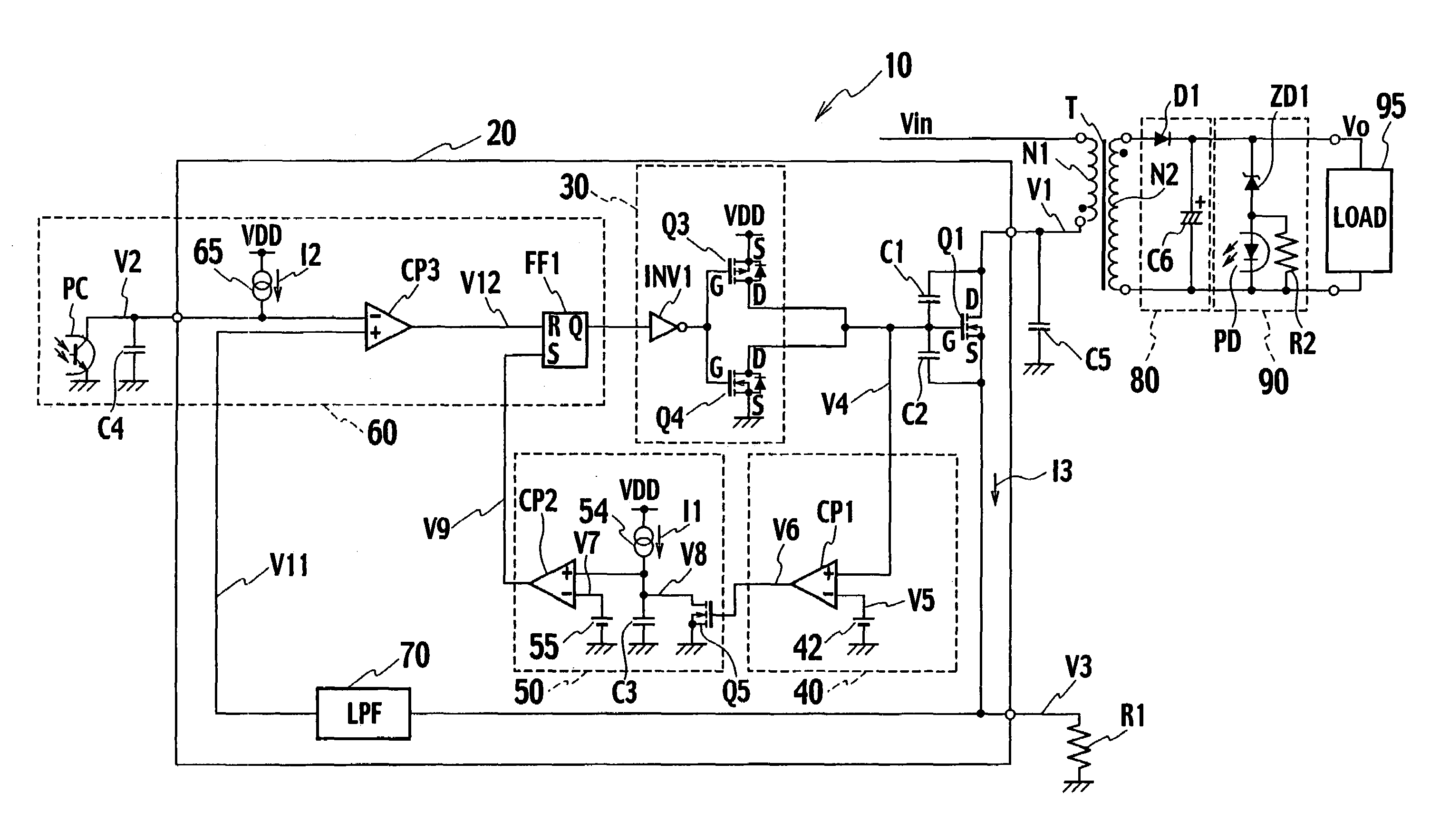
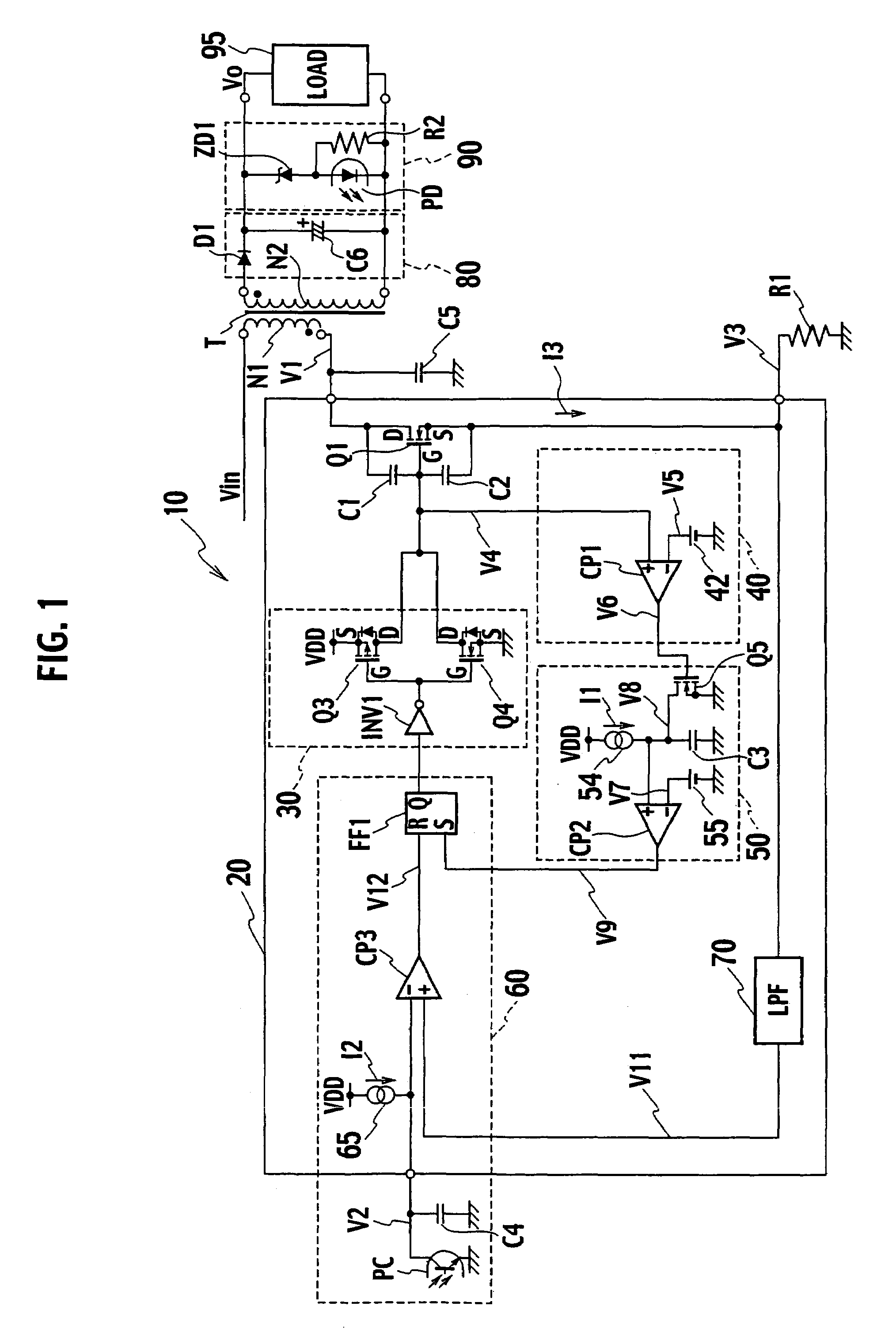
[0046]FIG. 3 shows a characteristic part of the first modification of the switching power source apparatus shown in FIG. 1.

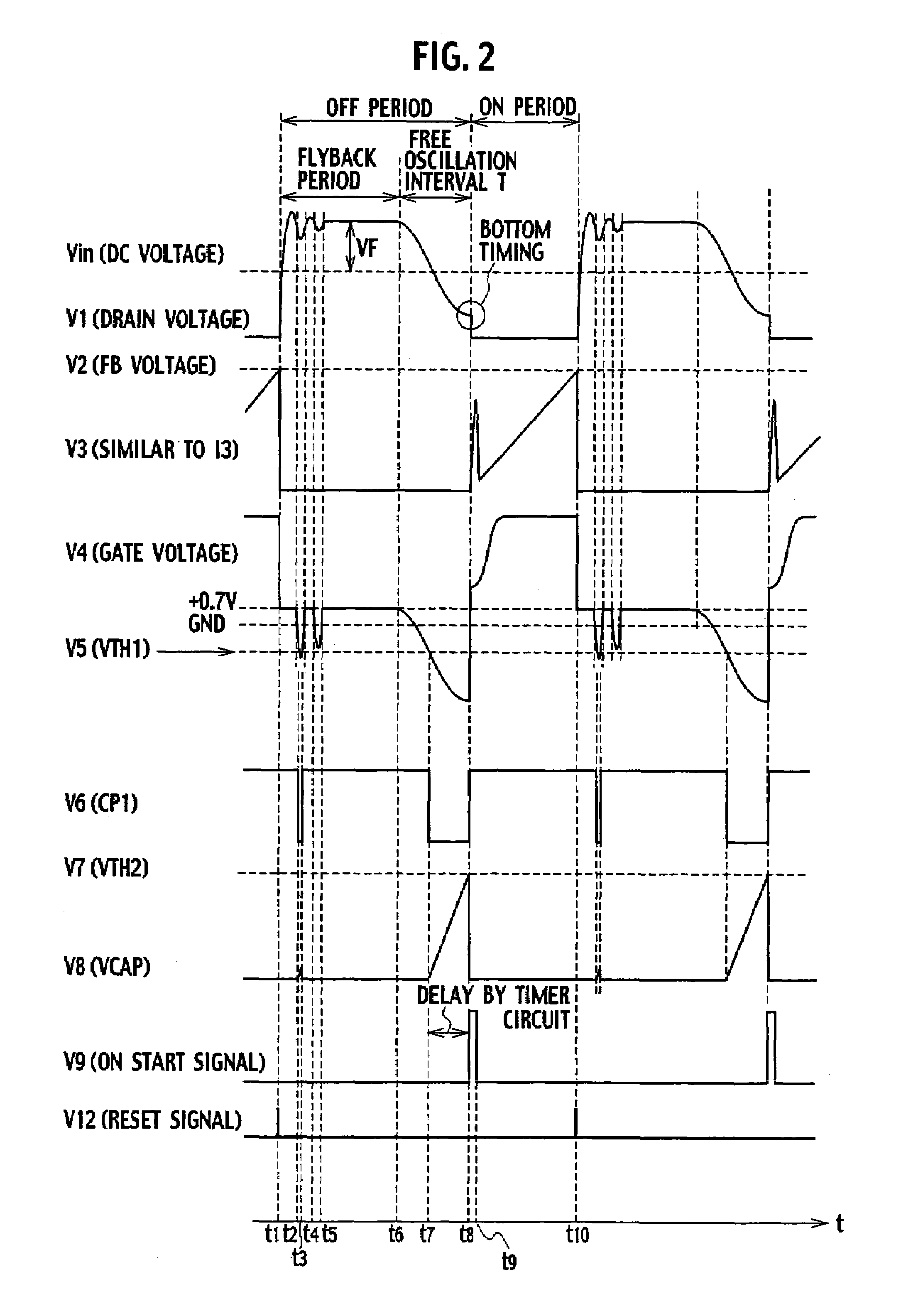
[0047]The first modification additionally arranges an impedance adjuster 100 between the driver 30. and the switching element Q1 of the configuration of FIG. 1. The impedance adjuster 100 provides a high impedance during an OFF period of the switching element Q1, to increase an amplitude voltage of parasitic oscillation occurring at the gate of the switching element Q1 after a flyback period.

[0048]In the configuration with the impedance adjuster 100, the drain of the drive element Q3 made of a p-type MOSFET is directly connected to the gate of the switching element Q1, the drain of the drive element Q4 made of an n-type MOSFET is connected through a resistor R3 to the gate of the switching element Q1, and the gate of the switching element Q1 is connected to the positive input terminal of the comparator CP1.

[0049]Operation of the impedance adjuster 100 will be ex...

second modification

[0052]FIG. 4 shows a characteristic part of the second modification of the switching power source apparatus shown in FIG. 1.

[0053]The second modification additionally arranges an impedance adjuster 110 between the driver 30 and the switching element Q1 of the configuration of FIG. 1. The impedance adjuster 110 selectively provides a high impedance during an OFF period of the switching element Q1 to increase an amplitude voltage of parasitic oscillation occurring at the gate of the switching element Q1 after a flyback period.

[0054]In the configuration with the impedance adjuster 110, the drain of the drive element Q3 made of a p-type MOSFET is directly connected to the gate of the switching element Q1, the drain of the drive element Q4 made of an n-type MOSFET is connected to a cathode of a Zener diode ZD2, an anode of the Zener diode ZD2 is connected to the gate of the switching element Q1, and the gate of the switching element Q1 is connected to the positive input terminal of the c...

third modification

[0062]FIG. 6 shows a characteristic part of the third modification of the switching power source apparatus shown in FIG. 1.

[0063]The third modification additionally arranges an impedance adjuster 120 between the driver 30 and the switching element Q1 of the configuration of FIG. 1. The impedance adjuster 120 selectively provides a high impedance during an OFF period of the switching element Q1, to increase an amplitude voltage of parasitic oscillation occurring at the gate of the switching element Q1 after a flyback period.

[0064]In the configuration with the impedance adjuster 120, the drain of the drive element Q3 made of a p-type MOSFET is directly connected to the gate of the switching element Q1, the drain of the drive element Q4 made of an n-type MOSFET is connected to a cathode of a diode D4, an anode of the diode D4 is connected to the gate of the switching element Q1, the gate of the switching element Q1 is connected to a cathode of a diode D5, an anode of the diode D5 is co...


PUM


Abstract

A switching power source apparatus has a switching element Q1. Between terminals of the switching element Q1, there is parasitic capacitance (C1, C2). A voltage V4 of parasitic oscillation appears at a gate of the switching element Q1 after a flyback period. A voltage detector detects a drop in the voltage V4 and outputs a detection signal V6. The detection signal V6 is delayed by a timer, which outputs an ON start signal synchronized with timing T at which the voltage V4 reaches a bottom level. In response to the ON start signal from the timer, a controller outputs an ON control signal to turn on the switching element Q1. In response to the ON control signal from the controller, a driver applies a drive signal to the gate of the switching element Q1, thereby driving the switching element Q1.

Description

BACKGROUND OF THE INVENTION[0001]1. Field of the Invention[0002]The present invention relates to a switching power source apparatus based on a quasi-resonance control method, capable of reducing package size and cost.[0003]2. Description of the Related Art[0004]The quasi-resonance control method is one of methods for controlling a switching power source apparatus having a switching element. During an OFF period of the switching element, a voltage of free oscillation due to parasitic oscillation at a drain of the switching element drops. When the voltage drop reaches a bottom level, the quasi-resonance control method detects it and turns on the switching element. This method can reduce a switching loss and noise. The method is disclosed in, for example, Japanese Patent Publication No. 3022246.[0005]A switching power source apparatus proposed in the above-mentioned patent publication has a primary circuit connected to a primary winding of a transformer, a secondary circuit connected t...

Claims


Application Information

Patent Timeline
Patent Type & Authority Patents(United States)
IPC IPC(8): H02M3/335H02H7/122
CPCH02M3/33507H03K17/165H03K17/6872H02M3/28H02M3/335
Inventor NAKAMURA, MASARU
Owner SANKEN ELECTRIC CO LTD
Why Eureka
Try Eureka