Apparatus and method for diagnosing integrated circuit

a technology of integrated circuits and diagnostic methods, applied in the direction of error detection/correction, power supply testing, instruments, etc., can solve the problems of large increase in complexity of creation of test patterns, lsi is called, and defects inside lsi, so as to shorten the test time for the integrated circuit, increase the number of scan paths, and accurately specify all scan paths

Inactive Publication Date: 2008-02-26
FUJITSU LTD
View PDF10 Cites 17 Cited by
  • Summary
  • Abstract
  • Description
  • Claims
  • Application Information

AI Technical Summary

Benefits of technology

[0022]In the light of the above problems, an object of the present invention is to provide a technique, which can not only detect a manufacturing failure (fault) of an integrated circuit but also specify a position at which the failure occurs even when outputs from scan paths are compressed and stored, or the number of scan paths is large.
[0032]Since a plurality of outputs shifted out from a plurality of shift registers are enabled one by one, and the enabled outputs are compressed by the EOR (exclusive OR) tree circuit and successively outputted to the outside, it is possible to accurately specify all scan paths in which faults exist when fault diagnosis is made on an LSI under test such as BIST OR the like. Even when a number of faults concurrently exist because a new manufacturing process is started, accurate, certain fault diagnosis is possible.
[0033]At this time, outputs from shift registers corresponding to patterns of pattern numbers in a predetermined range generated by the pattern generator are enabled, and the fault diagnosis is made. Whereby, it is possible to narrow down a pattern number where a fault occurs to specify a position of the fault in the scan path.
[0034]Test patterns generated by the pattern generator are modified by the pattern modifier and inputted to a plurality of shift registers (scan path). It is thereby possible to increase the number of the scan paths to decrease the number of the stages of the scan paths, thus largely shorten the test time for the integrated circuit. It is also possible to solve the problems with DSPT and BIST, and generate test patterns which provide advantages of the both and enable a high-quality test within a short time. At this time, only meaningful data (information on F / Fs required to be set values) is supplied from the tester (external input) and modified, which allows a large decrease in quality of the data to be stored in the tester. Therefore, a high-quality test becomes possible without imposing server design rules on the designer and without an expensive tester.
[0035]An indeterminate value in outputs from a plurality of shift registers formed with sequential circuit elements inside the integrated circuit is masked, and a masked output result is verified by the output verifier. It is thereby possible to prevent the compressed result from being ruined by the indeterminate state even if the output results from the sequential circuit elements are compressed and read out to the outside.

Problems solved by technology

Defect occurring inside an LSI due to a manufacturing failure of the LSI is called fault.
When the LSI includes sequential circuit elements [flip-flop (F / F), latch and RAM (Random Access Memory)], complexity of creation of test patterns is greatly increased.
When setting and reading are repetitively carried out for each test pattern in all sequential circuit elements forming scan paths in the above DSPT, not only the test time increases but also a problem occurs that the memory capacity of the tester lacks due to an increase in quantity of the test data.
Accordingly, execution of the test in DSPT becomes difficult.
Particularly, shortage of the memory capacity of the tester caused by an increase in quantity of test data largely raises the test cost because the memory has to be increased or the tester has to be upgraded.
Further, the BIST circuit can increase the speed of the shifting-in / shifting-out operation to the scan paths by increasing the number of the scan paths, thereby shortening the test time.
Although the above problem with the DSPT can be improved by employing BIST as above, there are still some problems.
Namely, a problem with BIST is the quality of the test (fault coverage) because a pseudo-random pattern is used therein.
When the MISR captures an indeterminate value (X value) even once, all registers in the MISR become the indeterminate state because of its structure, and values held in the registers are destroyed, which renders the test impossible.
These severe constraints in design are placed on the designer when the BIST is applied to a practical circuit.
Further, there is another problem that area overhead of the circuit or performance degradation occurs because of an additional circuit for BIST and insertion of a test point.
On the contrary, the BIST circuit shown in FIG. 7 or the test circuit shown in FIG. 8 compresses output results and stores them in the MISR of the output verifier 7, and reads out values in the MISR after the test is completed, so that the fault diagnosis is difficult.
Additionally, the number of scan paths is increased to increase the speed of the test in the test such as BIST or the like, so that outputs of all scan paths cannot be observed at external pins because of limitation of the number of pins of an LSI.
In other words, the fault diagnosis is impossible.

Method used


Image

  • Apparatus and method for diagnosing integrated circuit
  • Apparatus and method for diagnosing integrated circuit
  • Apparatus and method for diagnosing integrated circuit

Examples


first embodiment

[0045]1 Description of First Embodiment

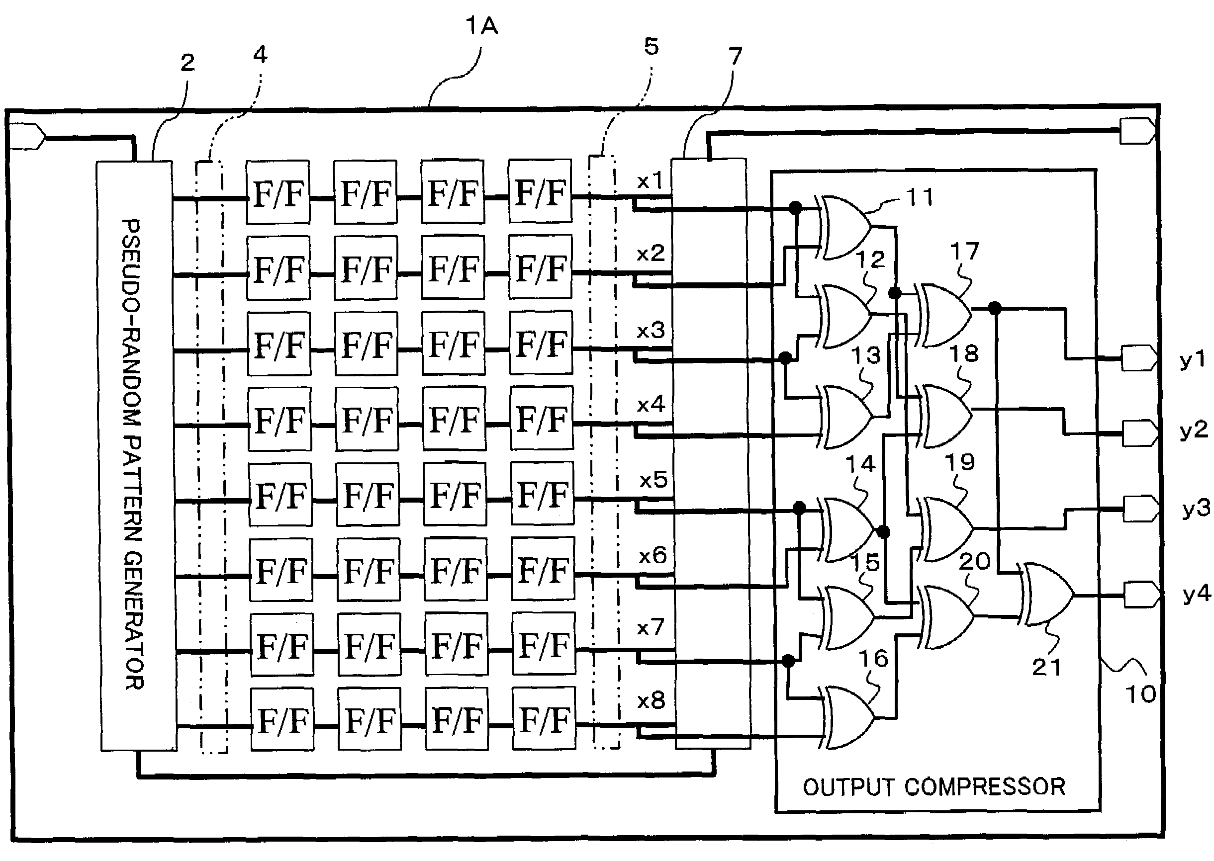
[0046]For fault diagnosis, agreement / disagreement information (information on whether a scan path output agrees with an expected value for each test pattern) for each test pattern is necessary, like DSPT. Since a scan path output is not compared with an expected value for each test pattern in BIST, it is necessary to read values of F / Fs for each test pattern to the outside. However, the number of inside parallel scan paths is increased for the purpose of a high-speed test in BIST, so that external output pins in number equal to all scan paths cannot be prepared because of limitation of the number of input / output pins of an LSI. Accordingly, some measures are necessary to compress information of a number of scan paths and observe it at a small number of external output pins. A first embodiment of this invention provides such measures.

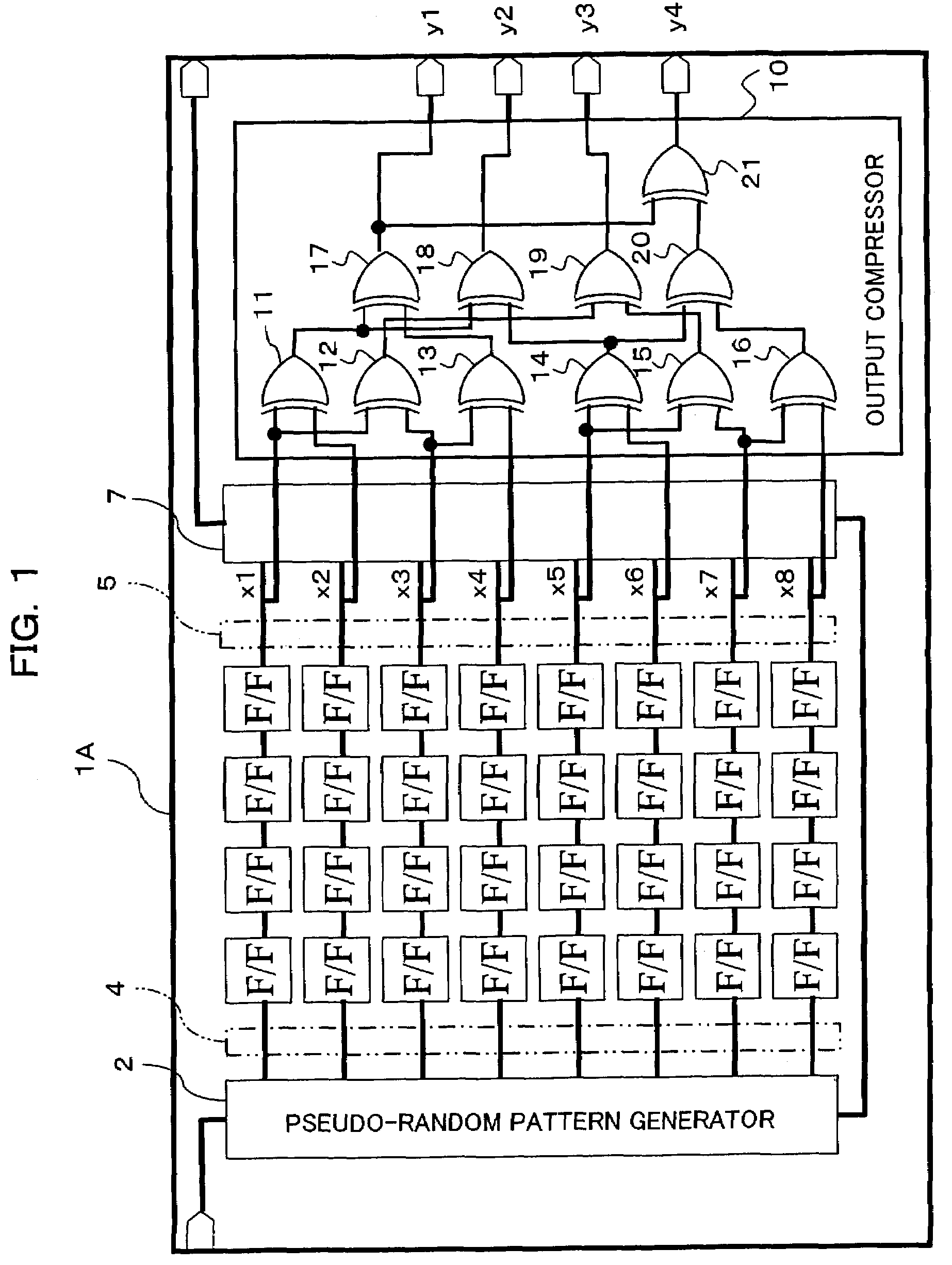
[0047]FIG. 1 is a block diagram showing a structure of a diagnosing apparatus for an integrated circuit according...

second embodiment

[0068]2 Description of Second Embodiment

[0069]When a plurality of faults concurrently occur, it is impossible to specify positions of the faults in the above first embodiment. This easily occurs when a new manufacturing process is started, thus necessity of fault diagnosis is large. According to second and third embodiments, it becomes possible to accurately specify all scan paths in which faults occur as necessary.

[0070]FIG. 3 is a block diagram showing a structure of a diagnosing apparatus for an integrated circuit according to the second embodiment of this invention. As shown in FIG. 3, the diagnosing apparatus according to the second embodiment comprises a pseudo-random pattern generator 2, a plurality of scan paths, and an output verifier 7 similar to those according to the first embodiment, along with an output selector 30 instead of the output compressor 10. The diagnosing apparatus is built in an LSI 1B that is an integrated circuit to be tested.

[0071]Like the LSI 1A accordi...

third embodiment

[0086]3 Description of Third Embodiment

[0087]FIG. 4 is a block diagram showing a structure of a diagnosing apparatus for an integrated circuit according to a third embodiment of this invention. As shown in FIG. 4, the diagnosing apparatus according to the third embodiment comprises a pseudo-random pattern generator (LFSR) 2, a plurality of scan paths (shift registers) and an output verifier (MISR) 7 similar to those according to the first or second embodiment, along with a pattern modifier 4 similar to that according to the first embodiment between the pseudo-random pattern generator 2 and the plural scan paths, and a mask 5 similar to that according to the first embodiment between the plural scan paths and the output verifier 7. The diagnosing apparatus is built in an LSI 1C that is an integrated circuit to be tested.

[0088]Like the LSI 1A according to the first embodiment, the LSI 1C includes a plurality of F / Fs (sequential circuit elements). In the LSI 1C, the F / Fs form a pluralit...


PUM


Abstract

An apparatus being able to not only detect a manufacturing defect of an integrated circuit but also specify a position at which the defect occurs even when outputs from scan paths are compressed and stored, or when the number of the scan paths is large. The apparatus has a pattern generator built in an integrated circuit to generate test patterns, a plurality of shift registers formed in parallel, into which the test patterns are shifted, and an output compressor for compressing a plurality of outputs shifted out from the shift registers with check bits of a Hamming code, and outputting them to the outside of the integrated circuit.

Description

BACKGROUND OF THE INVENTION[0001]1) Field of the Invention[0002]The present invention relates to an apparatus and a method for making fault diagnosis to detect a manufacturing failure (fault) of an integrated circuit such as an LSI (Large Scale Integration) or the like and specify a position at which the fault occurs, and an integrated circuit having a function of accomplishing the fault diagnosis.[0003]2) Description of the Related Art[0004]Detection of a manufacturing failure of an integrated circuit such as an LSI is done by applying an appropriate signal value to an input pin of the LSI using a tester (ATE; Automatic Test Equipment), and comparing a signal value appearing at the output pin with an expected result. The signal value applied to the input pin and the expected value to be appeared at the output pin are together called a test pattern.[0005]Defect occurring inside an LSI due to a manufacturing failure of the LSI is called fault. To verify all faults that may occur insi...

Claims


Application Information

Patent Timeline
Patent Type & Authority Patents(United States)
IPC IPC(8): G01R31/3183G01R31/40G01R31/28G01R31/3185H01L21/822H01L27/04
CPCG01R31/318547
Inventor HIRAIDE, TAKAHISA
Owner FUJITSU LTD
Why Eureka
Try Eureka