Circuit and method for on-chip jitter measurement

a jitter measurement and circuit technology, applied in the field of jitter measurement, can solve the problems of increasing the speed of digital circuitry, putting strenuous demands on pll designers, and few mechanisms implemented to monitor jitter

Active Publication Date: 2008-03-04
META PLATFORMS INC
View PDF20 Cites 27 Cited by
  • Summary
  • Abstract
  • Description
  • Claims
  • Application Information

AI Technical Summary

Problems solved by technology

In the last several decades, a rapid increase in the speeds of digital circuitry have put strenuous demands upon PLL designers.
One result of the fast increase in performance is that harmful noise parameters are becoming a relatively larger design problem.
However, in high volume production of PLLs there are very few mechanisms implemented to monitor jitter.

Method used


Image

  • Circuit and method for on-chip jitter measurement
  • Circuit and method for on-chip jitter measurement
  • Circuit and method for on-chip jitter measurement

Examples


Embodiment Construction

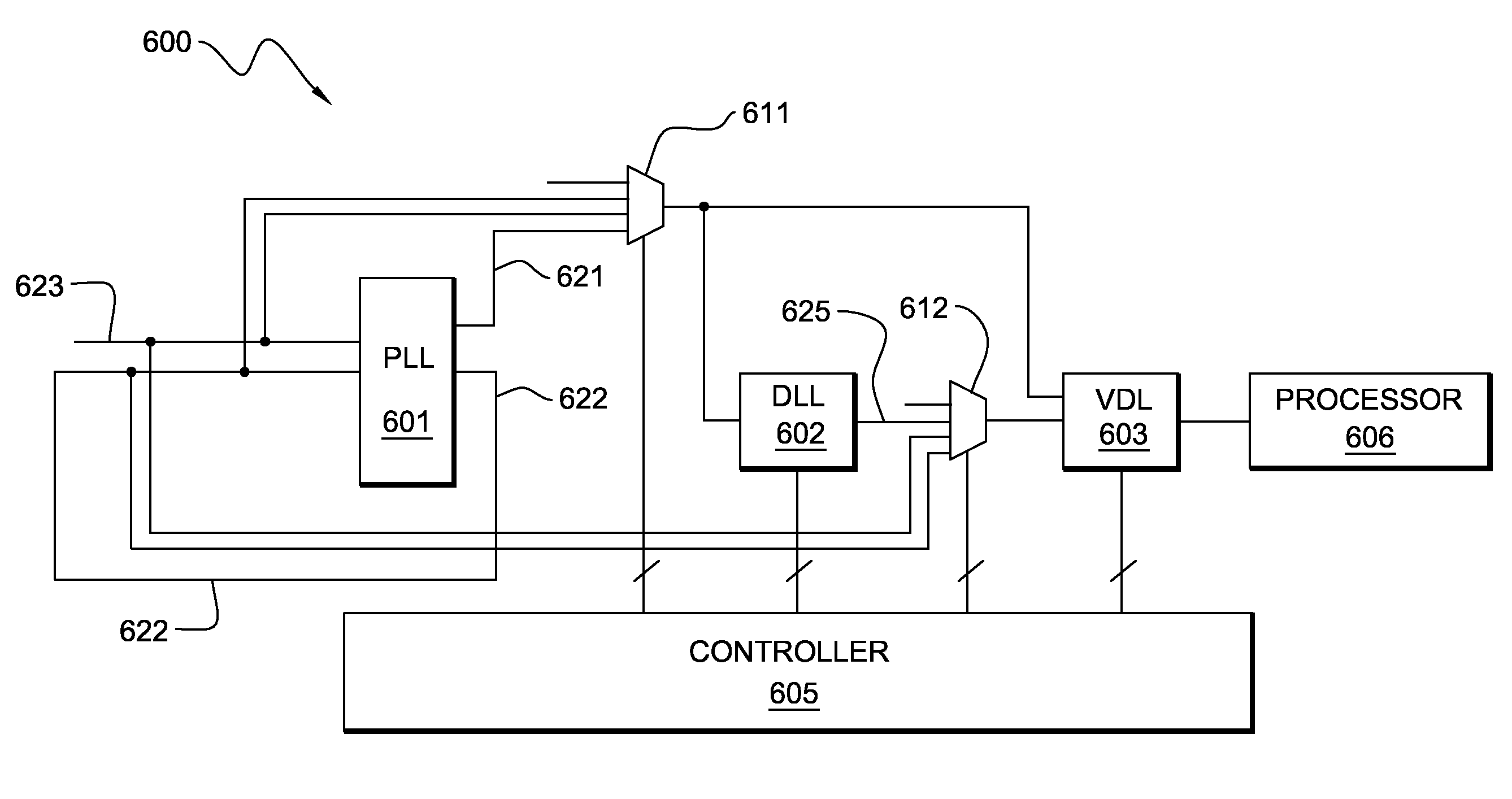
[0035]The embodiments of the invention and the various features and advantageous details thereof are explained more fully with reference to the non-limiting embodiments that are illustrated in the accompanying drawings and detailed in the following description. It should be noted that the features illustrated in the drawings are not necessarily drawn to scale. Descriptions of well-known components and processing techniques are omitted so as to not unnecessarily obscure the embodiments of the invention. The examples used herein are intended merely to facilitate an understanding of ways in which the embodiments of the invention may be practiced and to further enable those of skill in the art to practice the embodiments of the invention. Accordingly, the examples should not be construed as limiting the scope of the embodiments of the invention.

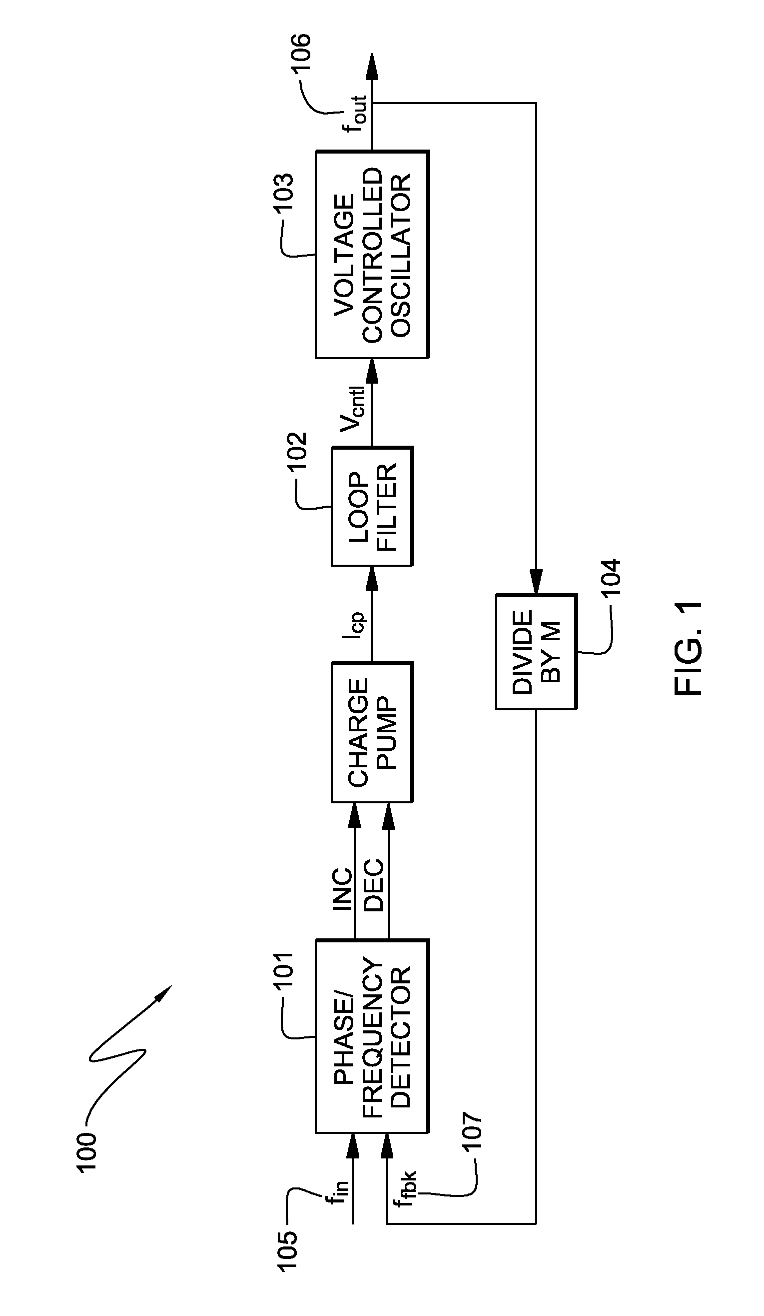
[0036]Phase locked loops (commonly referred to as PLLs) are found in a large number of computer, wireless, and communication systems with many d...


PUM


Abstract

An improved built-in self-test (BIST) circuit and an associated method for measuring phase and / or cycle-to-cycle jitter of a clock signal, the BIST circuit implement a Variable Vernier Digital Delay Locked Line method. Specifically, the embodiments of the BIST circuit incorporate both a digital delay locked loop and a Vernier delay line, for respectively coarse tuning and fine tuning portions of the circuit. Additionally, the BIST circuit is variable, as the resolution of the circuit changes from chip to chip, and digital, as it is implemented with standard digital logic elements.

Description

BACKGROUND[0001]1. Field of the Invention[0002]The embodiments of the invention generally relate to jitter measurement, and, more particularly, to a built-in self-test (BIST) circuit for measuring phase and / or cycle-to-cycle jitter of a clock signal.[0003]2. Description of the Related Art[0004]Phase locked loops (commonly referred to as PLLs) are found in a large number of computer, wireless, and communication systems with many different applications such as clock recovery, frequency synthesis and clock noise filtration. In the last several decades, a rapid increase in the speeds of digital circuitry have put strenuous demands upon PLL designers. One result of the fast increase in performance is that harmful noise parameters are becoming a relatively larger design problem. One such parameter, jitter, has quickly become one of the most critical parameters in specifying the operation of a PLL. As a result, extremely accurate analysis of PLL jitter characteristics is becoming required ...

Claims


Application Information

Patent Timeline
Patent Type & Authority Patents(United States)
IPC IPC(8): G01R23/175H03L7/06
CPCG01R29/26G01R31/31709H03L7/07H03L7/0814H03L7/0816H03L7/0818
Inventor KAM, BRANDON R.WYATT, STEPHEN D.
Owner META PLATFORMS INC
Why Eureka
Try Eureka