

Method and apparatus for generating layout pattern
a layout pattern and method technology, applied in the direction of computer aided design, cad circuit design, instruments, etc., can solve the problems of high probability of drawing errors in layout patterns, work that requires much effort and time, and high labor intensity of any method, so as to achieve rapid generation, reduce labor intensity, and avoid the probability of human operation errors
- Summary
- Abstract
- Description
- Claims
- Application Information
AI Technical Summary
Benefits of technology
Problems solved by technology
Method used
Image

Examples
first embodiment
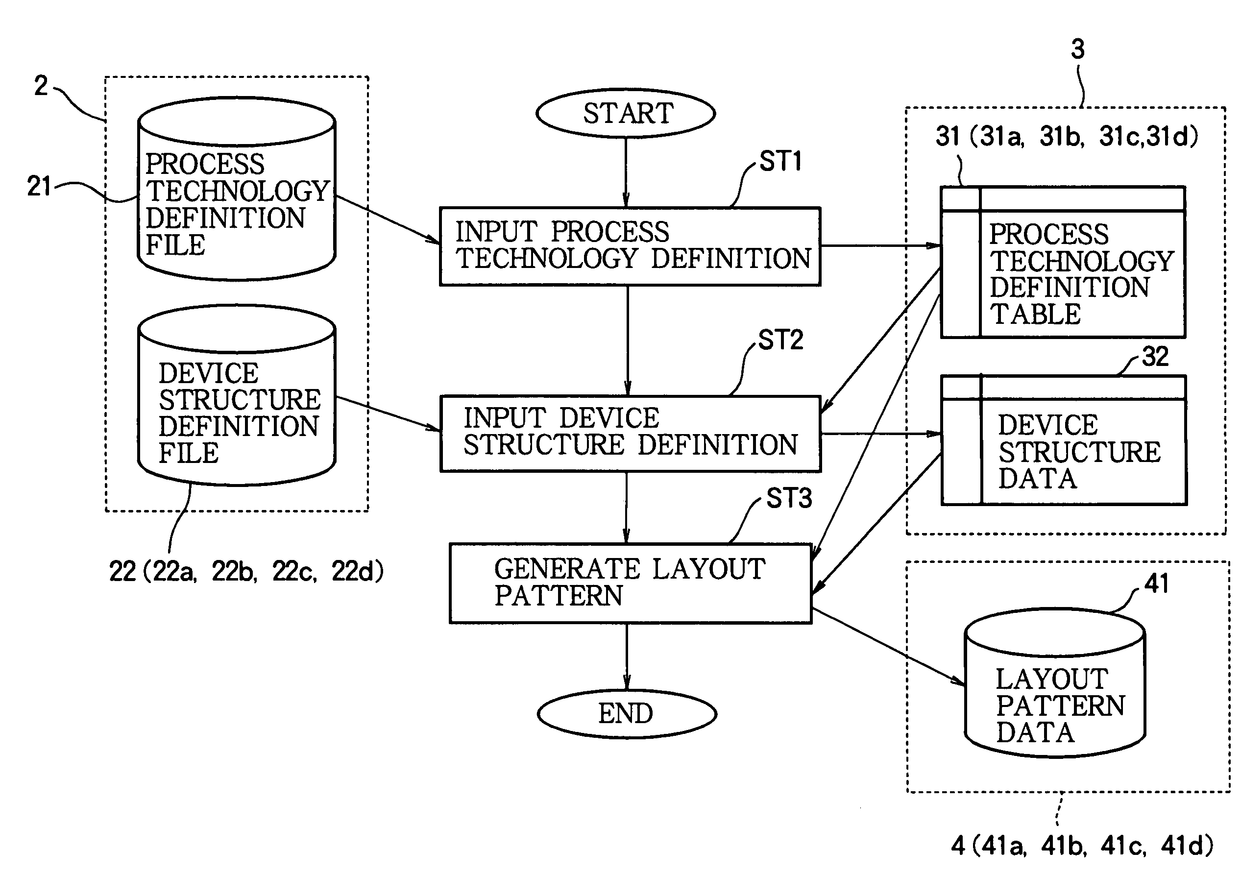
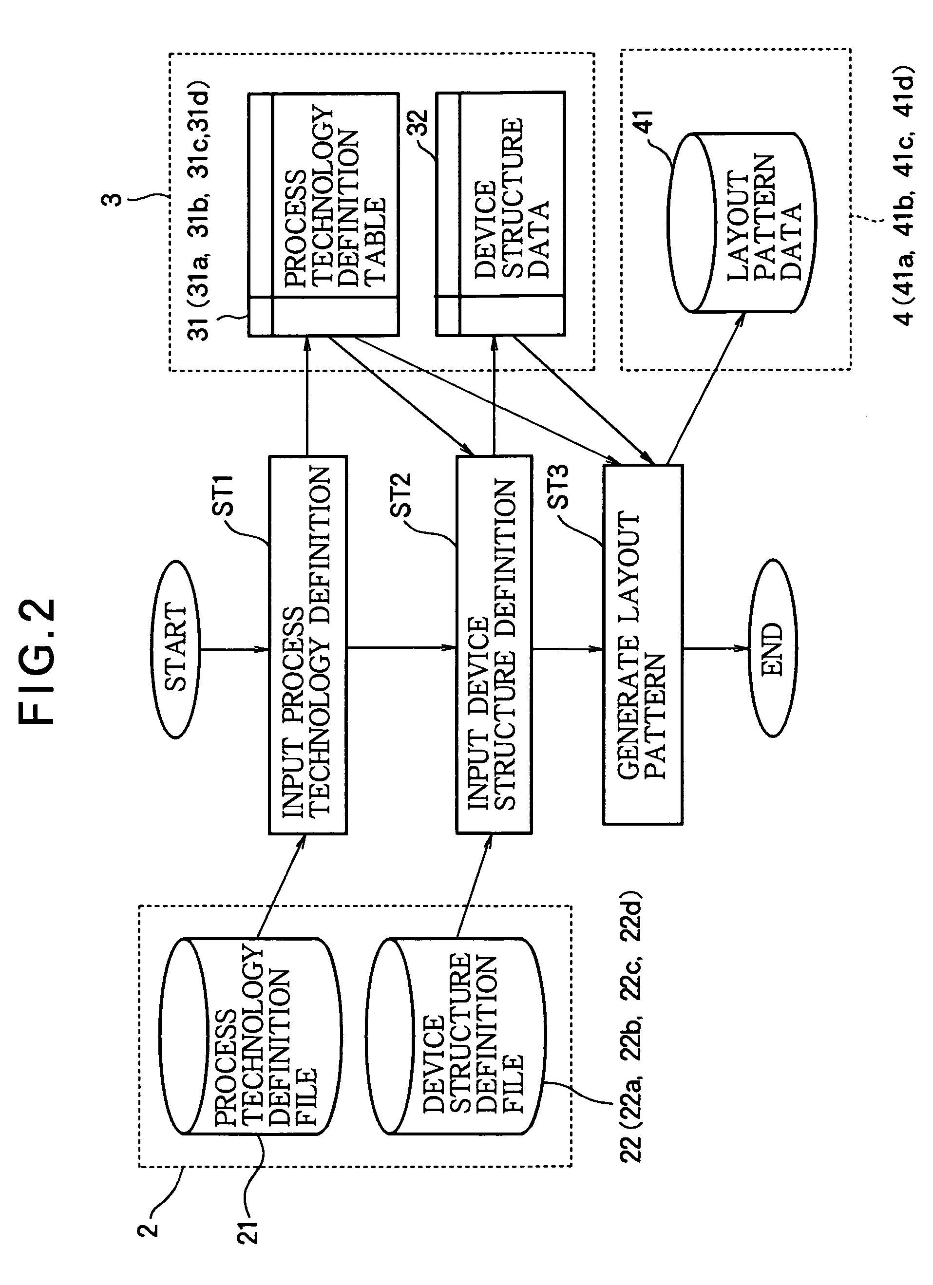
[0055]In the first embodiment, a case where a basic cell as an object, in which a layout pattern is generated or changed, is a transistor device will be described.
[0056]FIGS. 4A to 4E are diagrams showing sample device templates included in the device structure definition file to be used in the layout pattern generation method according to the first embodiment. As shown in FIGS. 4A to 4E, the device templates are divided into two types: a basic structure that is absolutely needed to generate the layout pattern of the transistor device (FIG. 4A) and an optional structure that are needed depending on the type of the transistor device (FIGS. 4B to 4E).
[0057]A device template 101 of the basic structure shown in FIG. 4A includes a gate layer (also referred to as “gate”) 111, an active layer (also referred to as “active”) 112, a contact layer (also referred to as “contact”) 113, and a metal layer (also referred to as “metal”) 114.
[0058]The width (e.g., W111 in FIG. 4A) of the gate layer 1...
second embodiment
[0085]In a second embodiment, a case where a basic cell as an object, in which a layout pattern is generated, is a resistor device will be described. In the second embodiment, the layout pattern of the resistor device can be automatically generated or changed by a method similar to the layout pattern generation method according to the first embodiment.
[0086]In the layout pattern generation method according to the second embodiment, the definition contents in the process technology definition file (21 in FIG. 2) are replaced with new definition contents of a resistor device file, and the new definition contents can be used to generate a layout pattern of the resistor device. In the process technology definition file (21 in FIG. 2), a drawing standard of a layer, a drawing standard between layers, a unit resistance of the resistor layer (layer structure “SheetResistor” forming the unit resistor of the basic cell in the row (f) of FIG. 3)-are created for all the layers forming the layo...
third embodiment
[0120]In the third embodiment, a case where a basic cell as an object, in which a layout pattern is generated, is a capacitor device will be described. In the third embodiment, the layout pattern of the resistor device can be automatically generated or changed in the similar way to in the layout pattern generation method according to the first or second embodiment.
[0121]In the layout pattern generation method according to the third embodiment, the definition of the process technology definition file (21 in FIG. 2) is first changed to a capacitor device file, and then the definition can be used to generate a layout pattern of a capacitor device. In the process technology definition file (21 in FIG. 2), a drawing standard of a layer, a drawing standard between layers, and a unit capacitor of the capacitor layer (i.e., a layer structure “AreaCapacitor” forming the unit capacitor of the basic cell in a row (g) of FIG. 3) are created for all the layers forming the layout pattern of the b...
PUM
 Abstract
Description
Claims
Application Information