Semiconductor device

a technology of semiconductor devices and electrode pads, applied in semiconductor devices, semiconductor/solid-state device details, electrical apparatus, etc., can solve the problems of increased chip size, resistance and inductance affecting circuit characteristics, and unnecessary gaps required for rewiring layout, etc., to facilitate the rewiring layout, economic effect, and efficient rewiring

Active Publication Date: 2008-03-11
ROHM CO LTD
View PDF5 Cites 18 Cited by
  • Summary
  • Abstract
  • Description
  • Claims
  • Application Information

AI Technical Summary

Benefits of technology

[0016]According to this aspect, the plurality of electrode pads are arranged between the first group of external electrodes and the second group of external electrodes. Consequently, the external electrodes included in either of the groups can be connected by approximately the same distances of rewiring. Since the lengths of the rewiring traces have an impact on the wiring resistances and inductances, it is possible to suppress variations in the electric characteristics. In addition, since the rewiring need not be routed outside the first group of external electrodes, it is possible to put the first group of external electrodes closer to the outer edges of the semiconductor device without constraints from the layout of the rewiring. This can suppress an increase in chip size.
[0018]The “input / output circuits” refer to protective elements which are connected with the respective electrode pads and protect internal circuit elements, and circuits which have a predetermined circuit configuration and size, such as an input / output buffer. Since the input / output circuits are disposed to the space above the integrated circuit, appearing outside the electrode pads, it is possible to improve the use efficiency of space. This allows a further reduction in chip size.
[0020]With twice the spacing in particular, two adjoining external electrodes out of the first group of external electrodes and two out of the second group of external electrodes are located near respective corresponding four electrode pads. This allows economic, efficient rewiring.
[0021]The first and second groups of external electrodes may be arranged systematically at regular intervals. The systematic arrangement of the external electrodes facilitates determining the layout of the electrode pads and the rewiring.
[0025]The plurality of electrode pads may be arranged linearly in parallel with the first and second rows of groups of external electrodes. Since the plurality of electrode pads are arranged linearly, the external electrodes and the electrode pads are situated in parallel with each other. This can simplify the rewiring connections.

Problems solved by technology

This causes differences in the rewiring length, which can adversely affect circuit characteristics including resistances and inductances.
Consequently, useless gaps required for the rewiring layout appear on the periphery of the semiconductor device 500 outside the solder bumps 20.
There has thus been the problem of an increased chip size.

Method used


Image

  • Semiconductor device
  • Semiconductor device
  • Semiconductor device

Examples


first embodiment

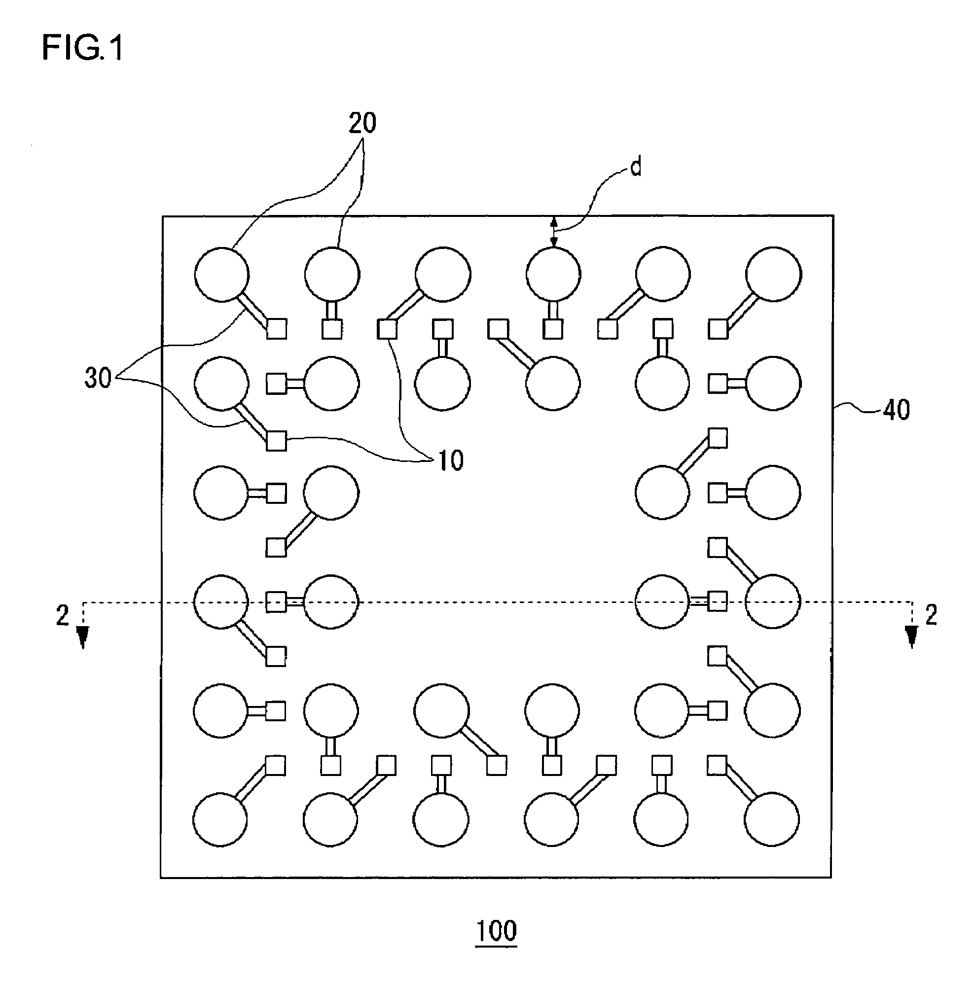
[0037]FIG. 1 is a diagram showing a semiconductor device 100 according to an embodiment of the present invention, as viewed from the electrode-pad side. The semiconductor device 100 has a CSP structure. In the diagram, the semiconductor device 100 includes: a plurality of electrode pads 10 for inputting and outputting signals from / to exterior; solder bumps 20 for making external lead electrodes; and rewiring 30.

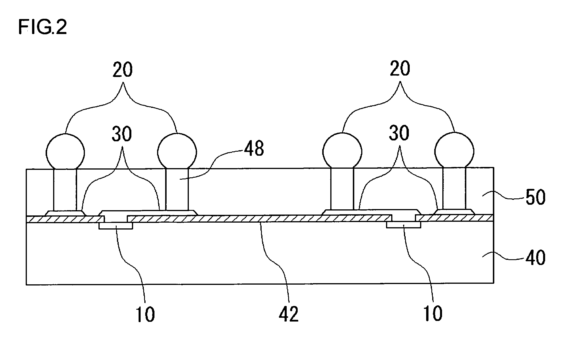
[0038]FIG. 2 is a sectional view taken along the line 2-2 of FIG. 1. This semiconductor device 100 has the WL-CSP structure in which external connection electrodes are formed directly on its semiconductor substrate 40. The semiconductor device 100 includes the semiconductor substrate 40, a protective film 42 for passivation, the electrode pads 10, the rewiring 30, posts 48, the solder bumps 20, and a sealing resin 50. Semiconductor integrated circuits including such devices as a transistor are formed on the top of the semiconductor substrate 40, and are provided with the elec...

second embodiment

[0043]The semiconductor device 100 according to this second embodiment is characterized by that the solder bumps 20 and the rewiring 30 are arranged systematically. FIGS. 3A to 3C show part of the layout of the electrode pads 10, the solder bumps 20, and the rewiring 30 on the semiconductor device 100 according to the present embodiment.

[0044]Each of the areas shown in FIGS. 3A to 3C represents one of four areas 300a to 300d having the same shapes, corresponding to the respective sides of a rectangular, shown by the broken lines in FIG. 3D. In FIGS. 3A to 3C, both the electrode pads 10 and the solder bumps 20 are arranged at regular intervals.

[0045]In FIGS. 3A and 3B, the solder bumps 20 are arranged linearly in two parallel rows at regular intervals. The electrode pads 10 are arranged linearly in the area interposed between the two rows of solder bumps. The electrode pads 10 are spaced at approximately ½ the spacing of the solder bumps 20.

[0046]With the traces of rewiring 30, the r...

third embodiment

[0052]The semiconductor device 100 according to a third embodiment provides a method of making effective use of the space above a semiconductor integrated circuit, appearing outside the electrode pads 10 in the first and second embodiments.

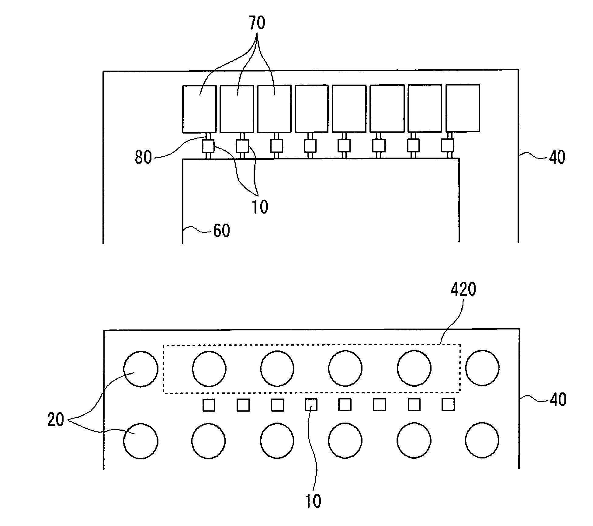
[0053]FIGS. 4A and 4B are plan views of part of the semiconductor device 100 according to the third embodiment, showing the layouts before and after packaging, respectively. As shown in FIG. 4A, before packaging, a semiconductor integrated circuit including the electrode pads 10, a functional circuit 60, and input / output circuits 70 is formed on the top of the semiconductor substrate 40. The electrode pads 10, the functional circuit 60, and the input / output circuits 70 are connected by ordinary wiring 80 inside the semiconductor integrated circuit.

[0054]The functional circuit 60 is a functional block for performing signal processing in the semiconductor integrated circuit. The functional circuit 60 varies in configuration and in area depending on ...


PUM


Abstract

The semiconductor device has the CSP structure, and includes: a plurality of electrode pads formed on a semiconductor integrated circuit in order to input / output signals from / to exterior; solder bumps for making external lead electrodes; and rewiring. The solder bumps are arranged in two rows along the periphery of the semiconductor device. The electrode pads are arranged inside the outermost solder bumps so as to be interposed between the two rows of solder bumps. Each trace of the rewiring is extended from an electrode pad, and is connected to any one of the outermost solder bumps or any one of the inner solder bumps.

Description

BACKGROUND OF THE INVENTION[0001]1. Field of the Invention[0002]The invention relates to a semiconductor device, and more particularly to a semiconductor device having a chip size package (hereinafter, referred to as CSP) structure.[0003]2. Description of the Related Art[0004]With the recent miniaturization of information terminals such as a cellular phone and a personal digital assistance (PDA), miniaturization of semiconductor devices to be used inside, such as LSIs, has been in increasing demand. Under such circumstances, attention has been given to a packaging technology called ball grid array (BGA) structure.[0005]Unlike conventional quad flat package (QFP) structures in which lead frames are used to connect semiconductor devices to a substrate, the BGA structure achieves substrate connection via terminals called solder bumps or solder balls which are formed on the surfaces of the semiconductor devices. According to this BGA structure, external connection terminals can be forme...

Claims


Application Information

Patent Timeline
Patent Type & Authority Patents(United States)
IPC IPC(8): H01L23/48
CPCH01L23/3114H01L24/10H01L24/13H01L24/14H01L2224/13099H01L2924/01013H01L2924/01029H01L2924/01079H01L2924/01082H01L2924/14H01L2924/19041H01L2924/30107H01L2924/01005H01L2924/01006H01L2924/01033H01L2924/014H01L2924/00H01L2224/13H01L2224/05144H01L2224/05147H01L2224/05644H01L2224/05647H01L2224/05124H01L2224/06135H01L2224/02377H01L2924/00014H01L24/06H01L2224/0401H01L2224/0612H01L2224/14104H01L23/50H01L23/528H01L23/53214H01L23/53228H01L23/53242H01L2224/13023H01L2224/13025H01L2224/1413
Inventor KOMIYA, KUNIHIRO
Owner ROHM CO LTD
Why Eureka
Try Eureka