Printed circuit board and method of manufacturing printed circuit board

a printed circuit board and printed circuit board technology, applied in the field of printed circuit boards, can solve the problems of insufficient effect of chip capacitors, inability to reduce wiring inductance as currently desired in the higher frequency region of ic chips, and inability to achieve the effect of enhancing connection characteristics, and reducing the probability of defective printed circuit boards

Inactive Publication Date: 2008-03-11
IBIDEN CO LTD
View PDF23 Cites 88 Cited by
  • Summary
  • Abstract
  • Description
  • Claims
  • Application Information

AI Technical Summary

Benefits of technology

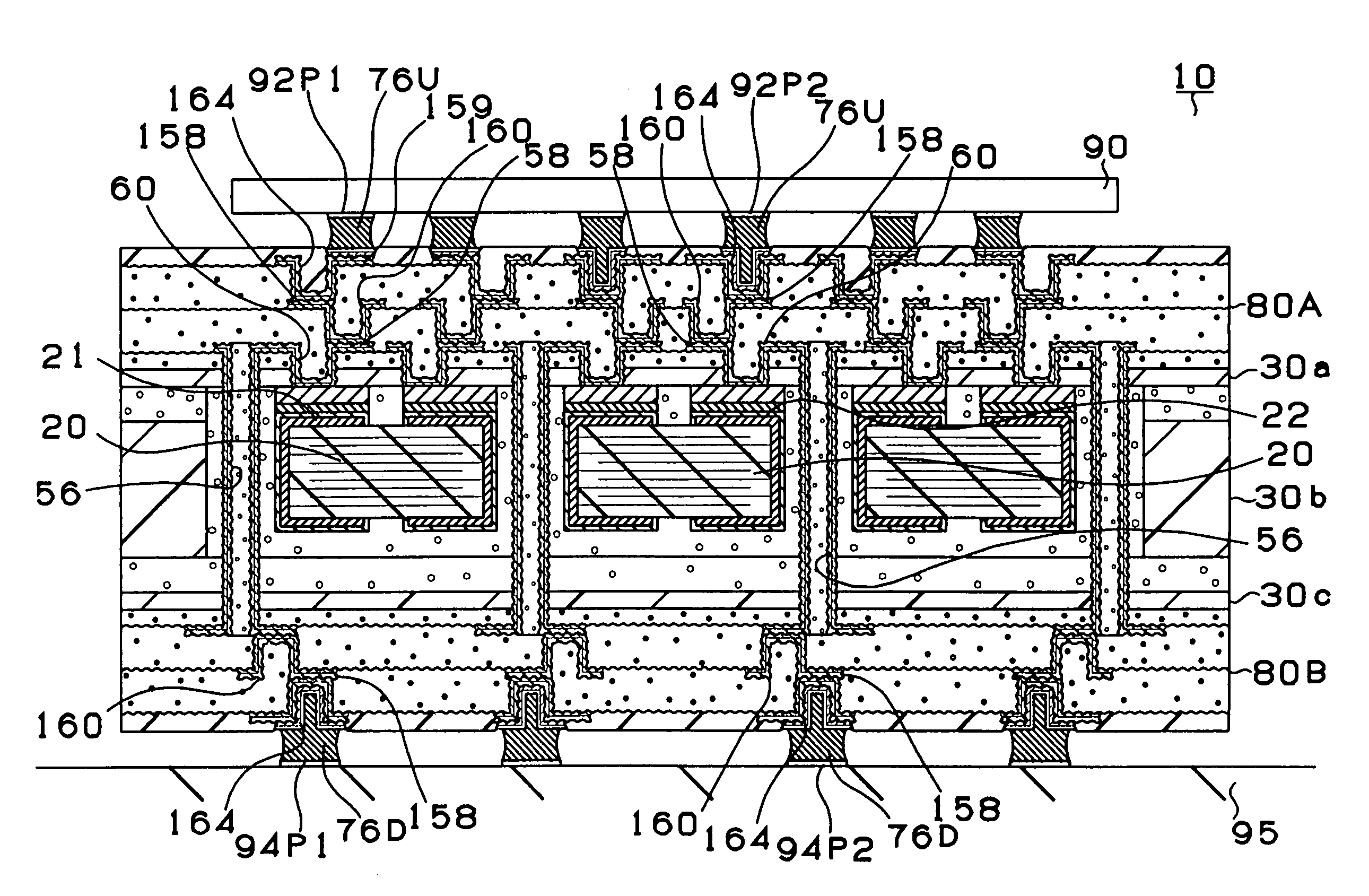
[0016]According to a printed circuit board recited in claim 1 and a printed circuit board manufacturing method recited in claim 16, the capacitor can be contained in the core substrate and the distance between the IC chip and the capacitor is shortened. Therefore, it is possible to reduce the loop inductance of the printed circuit board. Further, since the core substrate is constituted by providing resin substrates in a multilayer manner, it can obtain sufficient strength. Besides, since the core substrate is constituted smoothly by providing the first resin substrate and the third resin substrate on the both sides of the core substrate, respectively, it is possible to appropriately form interlayer resin insulating layers and conductor circuits on the core substrate and to thereby decrease the probability of the occurrence of defective printed circuit boards.
[0152]According to the invention recited in claim 72, upper surfaces of the plurality of capacitors within the concave portion are pressed or struck from above, thereby making heights of the upper surfaces of the capacitors uniform. Accordingly, in providing a plurality of capacitors within the concave portion, the heights of the capacitors can be made uniform and the core substrate can be made smooth even if the sizes of the plural capacitors are uneven. Thus, it is possible to appropriately form upper interlayer resin insulating layers and conductor circuits without hampering the smoothness of the core substrate, and, therefore, to decrease the probability of the occurrence of defective printed circuit boards.

Problems solved by technology

Due to this, as IC chip driving frequency increases, the chip capacitor cannot exhibit sufficient effect even if the chip capacitor is mounted on the surface of the printed circuit board.
However, according to the Publication Nos. 6-326472 and 7-263619 stated above, the distance from the IC chip to the capacitor cannot be set too short and the wiring inductance cannot be reduced as currently desired in the higher frequency region of the IC chip.
In case of a multi-layer buildup wiring board made of resin, in particular, due to the difference in the coefficient of thermal expansion and a capacitor made of ceramic and a core substrate as well as interlayer resin insulating layers made of resin, disconnection occurs between the terminal of the chip capacitor and a via, separation occurs between the chip capacitor and the interlayer resin insulating layers and cracks occur to the interlayer resin insulating layers.
Thus, the multi-layer buildup wiring board could not realize high reliability for a long time.
On the other hand, according to the invention of Publication No. 11-248311, if the position at which a capacitor is arranged is deviated, the connection between the terminal of the capacitor and a via cannot be accurately established and power cannot be possibly supplied from the capacitor to the IC chip.

Method used


Image

  • Printed circuit board and method of manufacturing printed circuit board
  • Printed circuit board and method of manufacturing printed circuit board
  • Printed circuit board and method of manufacturing printed circuit board

Examples


first embodiment

First Other Example of First Embodiment

[0267]A printed circuit board according to the first other example of the first embodiment of the present invention will be described hereinafter with reference to FIG. 9. The printed circuit board in the first other example of the first embodiment is almost the same as the printed circuit board in the first embodiment stated above. However, in the printed circuit board in the first other example, conductive connection pins 96 are provided at the printed circuit board and the printed circuit is connected to a daughter board through the conductive connection pins 96.

[0268]Further, in the first embodiment stated above, only the chip capacitors 20 contained in the core substrate 30 are provided. In this example, mass storage chip capacitors 86 are mounted on the front and reverse sides of the substrate.

[0269]The IC chip momentarily consumes high power and performs complex arithmetic operation. In the first other example, to supply high power to th...

second embodiment

[0296]The constitution of a printed circuit board according to the second embodiment of the present invention will be described hereinafter with reference to FIGS. 19 and 20. FIG. 19 is a cross-sectional view of a printed circuit board 210. FIG. 20 shows a state in which an IC chip 290 is mounted on the printed circuit board 210 shown in FIG. 19 and that the printed circuit board 210 is attached to a daughter board 295.

[0297]As shown in FIG. 19, the printed circuit board 210 consists of a core substrate 230 containing a chip capacitor 220, and buildup wiring layers 280A and 280B. The buildup wiring layers 280A and 280B are connected to each other by through holes 256. Each of the wiring layers 280A and 280B consists of interlayer resin insulating layers 240 and 340. At the upper buildup wiring layer 280A side, conductor circuits 358 and via holes 260 connected to the first electrode 221 and the second electrode 222 of the chip capacitor 220, respectively, are formed on the interlaye...

third embodiment

First Other Example of Third Embodiment

[0389]A printed circuit board according to the first other example of the third embodiment of the present invention will be described hereinafter with reference to FIG. 32. The printed circuit board in the first other example is almost the same as the printed circuit board in the third embodiment stated above. However, in the printed circuit board in the first other example, conductive connection pins 496 are provided at the printed circuit board and the printed circuit is connected to a daughter board through the conductive connection pins 496.

[0390]Further, in the third embodiment stated above, only the chip capacitors 420 contained in the core substrate 430 are provided. In this example, mass storage chip capacitors 486 are mounted on the front and reverse sides of the substrate.

[0391]The IC chip momentarily consumes high power and performs complex arithmetic operation. In the first other example, to supply high power to the IC chip, chip ca...


PUM

PropertyMeasurementUnit
thicknessaaaaaaaaaa
thicknessaaaaaaaaaa
temperatureaaaaaaaaaa

Abstract

A chip capacitor 20 is provided in a core substrate 30 of a printed circuit board 10. This makes it possible to shorten a distance between an IC chip 90 and the chip capacitor 20 and to reduce loop inductance. Since the core substrate 30 is constituted by providing a first resin substrate 30a, a second resin substrate 30b and a third resin substrate 30c in a multilayer manner, the core substrate 30 can obtain sufficient strength.

Description

[0001]This application is a divisional of U.S. Ser. No. 09 / 830,360 filed Apr. 25, 2001 now U.S. Pat. No. 6,724,638, which is the National Phase of International Application PCT / JP00 / 05970 filed Sep. 1, 2000. The entire contents of these applications are incorporated herein by reference.TECHNICAL FIELD[0002]The present invention relates to a printed board for mounting thereon electronic components such as an IC chip and a method of manufacturing the printed board. More particularly, the present invention relates to a printed circuit board including therein a capacitor or the like and a method of manufacturing the printed circuit board.BACKGROUND ART[0003]At present, for the purpose of smoothly supplying electric power to an IC chip, a chip capacitor is often mounted on the surface of a printed circuit board used as a package substrate.[0004]The reactance of a wiring from the chip capacitor to the IC chip depends on frequency. Due to this, as IC chip driving frequency increases, the c...

Claims


Application Information

Patent Timeline
Patent Type & Authority Patents(United States)
IPC IPC(8): H05K1/18H01L21/48H01L23/498H01L23/50H01L23/64H01L25/16H05K1/02H05K3/46
CPCH01L21/4857H01L23/49822H01L23/49827H01L23/50H01L23/642H01L23/645H01L24/16H01L24/17H01L25/16H01L25/162H05K1/0231H05K1/185H05K1/186H05K1/187H05K3/4602H05K1/181H01L2224/13099H01L2224/16H01L2224/82039H01L2224/82047H01L2924/01011H01L2924/01012H01L2924/01013H01L2924/01018H01L2924/0102H01L2924/01025H01L2924/01027H01L2924/01029H01L2924/0103H01L2924/01033H01L2924/01046H01L2924/01051H01L2924/01052H01L2924/01058H01L2924/01074H01L2924/01078H01L2924/01079H01L2924/01082H01L2924/14H01L2924/15311H01L2924/15312H01L2924/19041H01L2924/19105H01L2924/30105H01L2924/30107H01L2924/3011H05K3/4611H05K2201/0187H05K2201/09509H05K2201/09536H05K2201/10636H05K2201/10674H05K2203/063H01L2924/01005H01L2924/01006H01L2924/01019H01L2924/01023H01L2924/01043H01L2924/01047H01L2924/014H01L2224/16225H01L2924/07802H01L2224/16235Y10T29/4913Y10T29/49165Y10T29/49146Y10T29/49155Y10T29/435Y10T29/49117Y10T29/49126H01L2924/00H01L2224/05568H01L2224/05573H01L2924/00014H01L2924/12042H01L2924/13091H01L2924/181H01L2924/3511Y02P70/50H01L2224/05599H05K1/18
Inventor INAGAKI, YASUSHIASAI, MOTOOWANG, DONGDONGYABASHI, HIDEOSHIRAI, SEIJI
Owner IBIDEN CO LTD
Why Eureka
Try Eureka