
Method and apparatus for purification of crystal material and for making crystals therefrom and use of crystals obtained thereby

a technology of crystal material and crystal material, which is applied in the direction of crystal growth process, instruments, melt solutions, etc., can solve the problems of poor image formation, increase the loss of chip production, etc., and achieve radiation resistance and laser damage in these crystals, scattering and absorption in the crystals made, and the effect of improving radiation resistance and laser damag

Inactive Publication Date: 2008-03-18
HELLMA MATERIALS
View PDF22 Cites 5 Cited by
  • Summary
  • Abstract
  • Description
  • Claims
  • Application Information

AI Technical Summary

Benefits of technology

"The present invention provides a method and apparatus for preparing large single crystals with low extrinsic absorption properties. The method involves optimizing process parameters during drying, scavenging, and homogenizing the melt, and utilizing a closable vessel for melting the crystal raw material. The resulting single crystals have reduced oxygen content and small diffuse scattering properties, and improved optical and electronic components can be made from them. The invention also provides a method for purifying the crystals by removing impurities, especially oxides, from the melt. The purification step involves reacting the impurities with scavengers, which can be PbF2, ZnF2, or SnF2 with alkali and alkaline earth halides, and the amount of scavenger used can be controlled to achieve a desired level of purity. The method and apparatus of the invention can produce high-quality single crystals with improved properties, and can be used for a variety of optical and electronic applications."

Problems solved by technology

Thus for example, crystal dislocations and especially schlieren formation or other defocusing structures in the photolithographic imaging circuitry, which can lead to short circuits and thus malfunction of the entire computer chip with increasing miniaturization, enormously increase the losses during chip production.
Also the heat generated by absorption at impurity and defect sites leads to thermal expansion of the optical elements during photolithography and thus to focal point changes, which similarly lead to poorer image formation.

Method used


Image

  • Method and apparatus for purification of crystal material and for making crystals therefrom and use of crystals obtained thereby
  • Method and apparatus for purification of crystal material and for making crystals therefrom and use of crystals obtained thereby
  • Method and apparatus for purification of crystal material and for making crystals therefrom and use of crystals obtained thereby

Examples


example 1

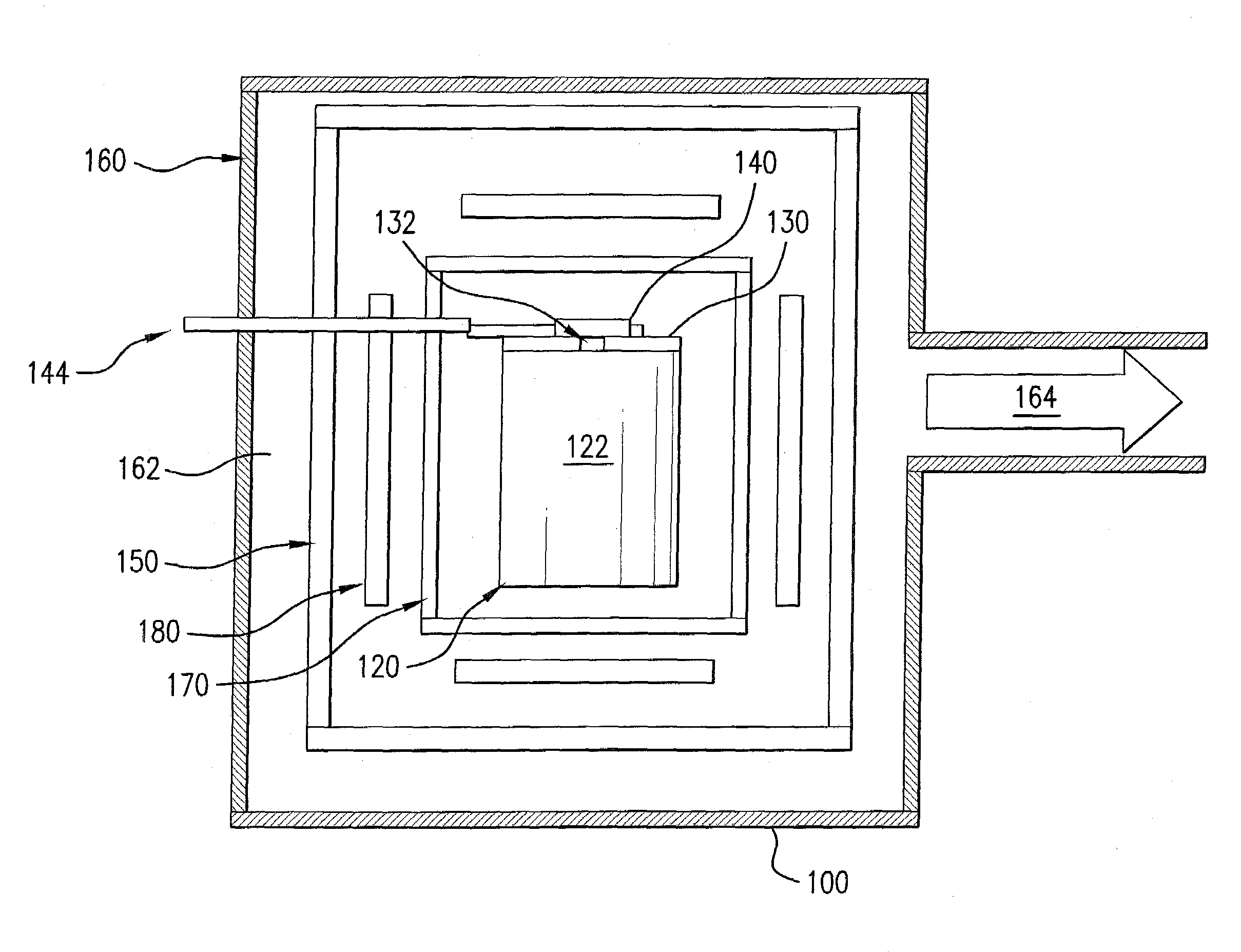
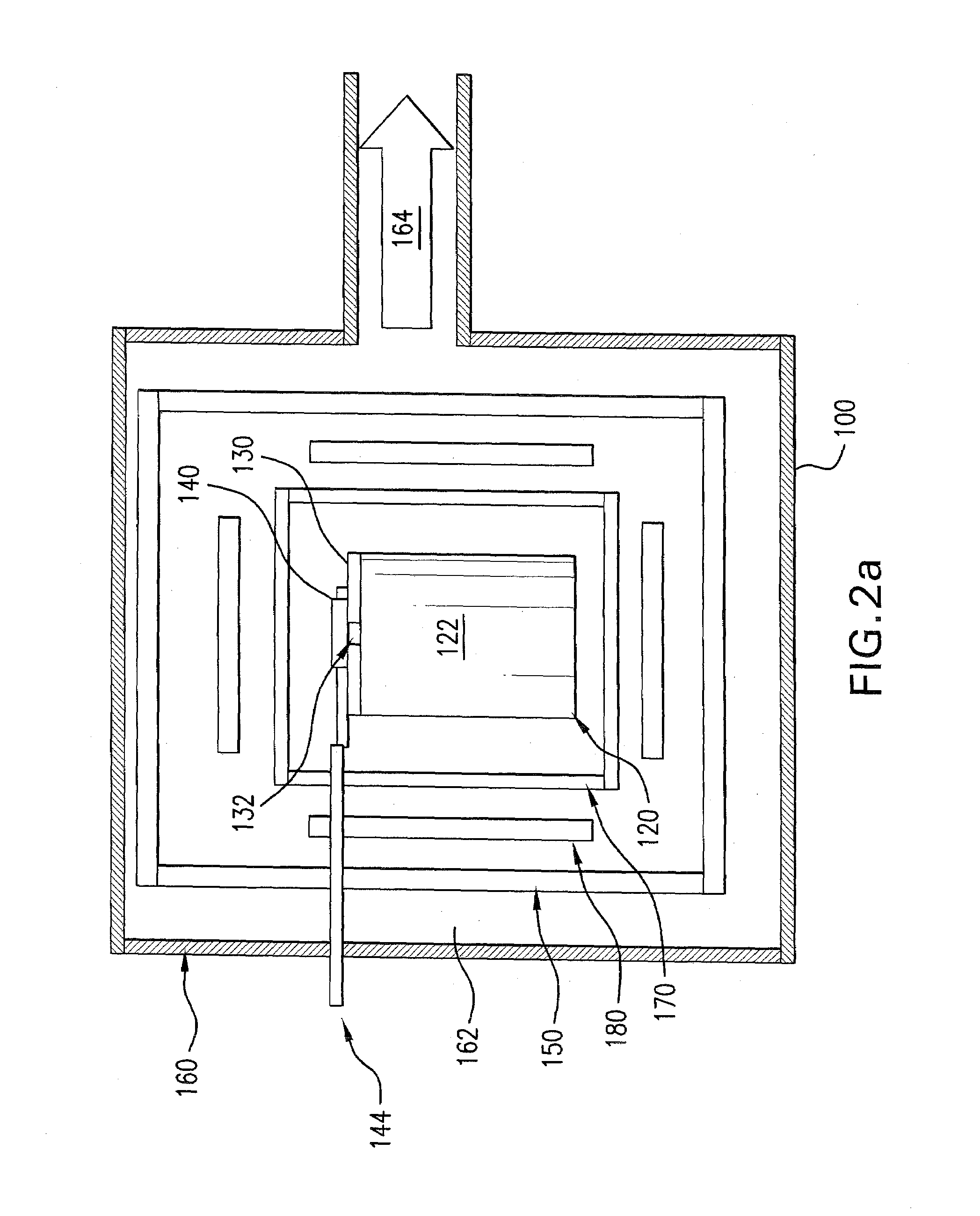
[0034]In a melt vessel 60 kg of high purity synthetic calcium fluoride powder, in which cationic impurities typically were less than 1 ppm, were mixed uniformly with 1 percent by weight of PbF2 (typical amounts are 0.5 to 3 percent by weight). The melt vessel 120 was closed by means of a vessel cover 130 having an opening 132. A plate-shaped sliding mechanism for closing the opening was arranged on the vessel cover. The mechanism included passages or through-going holes 142a, 142b, 142c with respective radii of 4 mm, 0.15 mm and 1.2 mm and lengths of 10 mm, which corresponded to the different geometric conductance values of 24.7461 mm2, 0.0025 mm2 and 1.0195 mm2. After filling and closing the melt vessel a vacuum of 0.9*10−3 Pa (0.9*10−5 mbar) was produced at the vessel exterior and one of the through-going holes was arranged to coincide with the vessel opening 132. Subsequently the temperature was increased to 700° C. and increased from there with a heating rate of 12° C. per hour ...


PUM

PropertyMeasurementUnit
temperatureaaaaaaaaaa

Abstract

The method for producing single crystals includes drying crystal raw material by removing water, reaction of impurities with a scavenger, preferably a metal halide, and homogenizing the melt. The method is performed with the raw material in a melt vessel with a variable-sized through-going opening, in which drying occurs at 100° C. to 600° C. for at least 20 hours with a geometric conductance value for the through-going opening of 2.00 to 30.00 mm2; the reacting occurs at 600° C. to 1200° C. for at least nine hours with a geometric conductance value of 0.0020 to 0.300 mm2 and the homogenizing occurs at above 1400° C. for at least six hours with a geometric conductance value of 0.25 to 1.1 mm2. Alternatively the geometric conductance value is the same during drying, reacting and homogenizing and takes a value between 0.25 and 1 mm2.

Description

BACKGROUND OF THE INVENTION[0001]1. Field of the Invention[0002]The present invention relates to a method for purification or refining crystal material, especially highly pure crystal raw material, for making crystals with less optical extrinsic absorption, especially by a multi-step treatment process for further purifying the raw material. It also relates to an apparatus for performing this method, which has a closable melt vessel with at least one closable opening and also to the use of the crystals obtained with this method.[0003]2. Related Art[0004]Crystals, especially single crystals, are increasingly used for making optical elements, such as lenses, etc. Many such crystals are used for high energy, especially short wavelength, radiation transmission and thus are suitable for making optical systems, such as lasers. They are also used in microlithography for manufacture of circuitry in small electrical components, such as computer chips. Not only ever larger sizes or geometries ...

Claims


Application Information

Patent Timeline
Patent Type & Authority Patents(United States)
IPC IPC(8): C30B11/02C30B11/00C30B29/12C30B33/00G02B1/02
CPCC30B11/00C30B29/12G02B1/02C30B33/00Y10T117/108Y10T117/1072
Inventor KANDLER, JOERGPARTHIER, LUTZKAUFHOLD, THOMASWEHRHAN, GUNTHERKUNISCH, CLEMENS
Owner HELLMA MATERIALS
Learn More