Helium-based etch process in deposition-etch-deposition gap fill

a technology of etching and helium, which is applied in the field of etching process for forming dielectric layers, can solve the problems of reducing budgets, increasing difficulty in void-free filling of narrow width, and not being entirely diffusion-based, so as to reduce the etch rate and alter the character of the etch

Active Publication Date: 2008-03-18
NOVELLUS SYSTEMS
View PDF112 Cites 26 Cited by
  • Summary
  • Abstract
  • Description
  • Claims
  • Application Information

AI Technical Summary

Benefits of technology

[0007]The present invention addresses this need by providing chemical vapor deposition and biased etch back processes that replace fluorine-based etchants with a helium-based etch chemistry. He is the major or only component of the etch process chemistry and primary or only etchant. The etch process chemistry may also include an inert carrier gas, such as Ar or N2, and / or an etch process modulator, such as a minor component of H2 or O2. The process modulating gases may alter the character of the etch, such as by stabilizing the plasma or reducing the etch rate.

Problems solved by technology

As device geometries shrink and thermal budgets are reduced, void-free filling of narrow width, high aspect ratio (AR) spaces (e.g., AR>3:1) becomes increasingly difficult due to limitations of existing deposition processes.
Thus, HDP CVD is not an entirely diffusion-based (isotropic) process.
However, the application of those etchants may contaminate the dielectric (e.g., STI) film with foreign atoms, e.g., C, N and F, causing issues in the subsequent integration processes and device degradation.

Method used


Image

  • Helium-based etch process in deposition-etch-deposition gap fill
  • Helium-based etch process in deposition-etch-deposition gap fill
  • Helium-based etch process in deposition-etch-deposition gap fill

Examples


Embodiment Construction

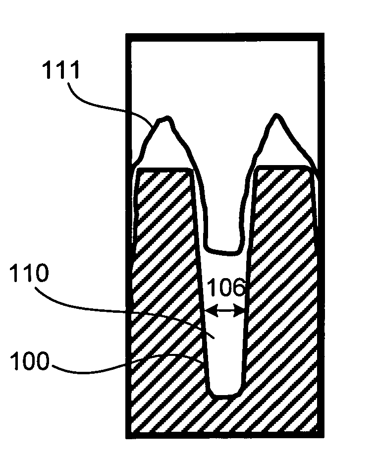
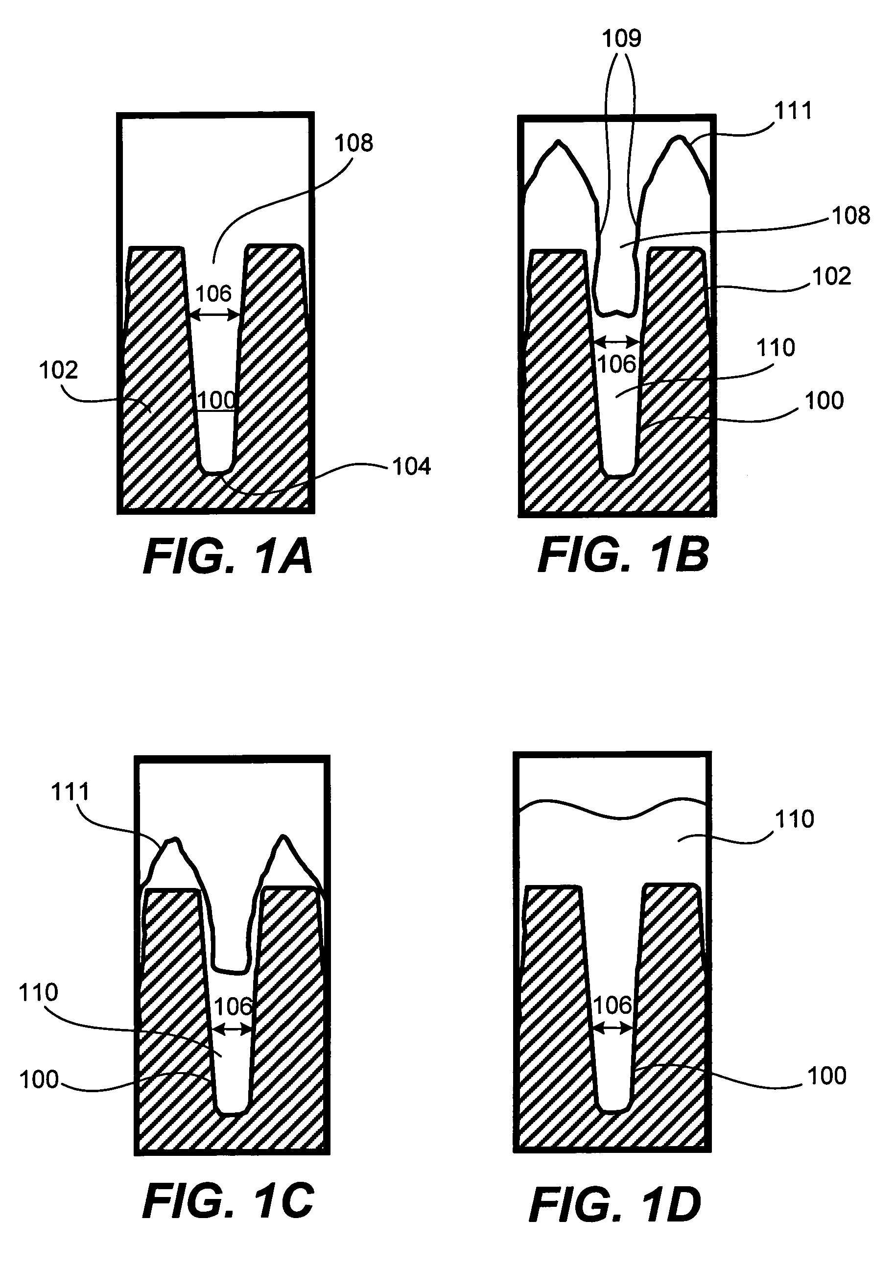
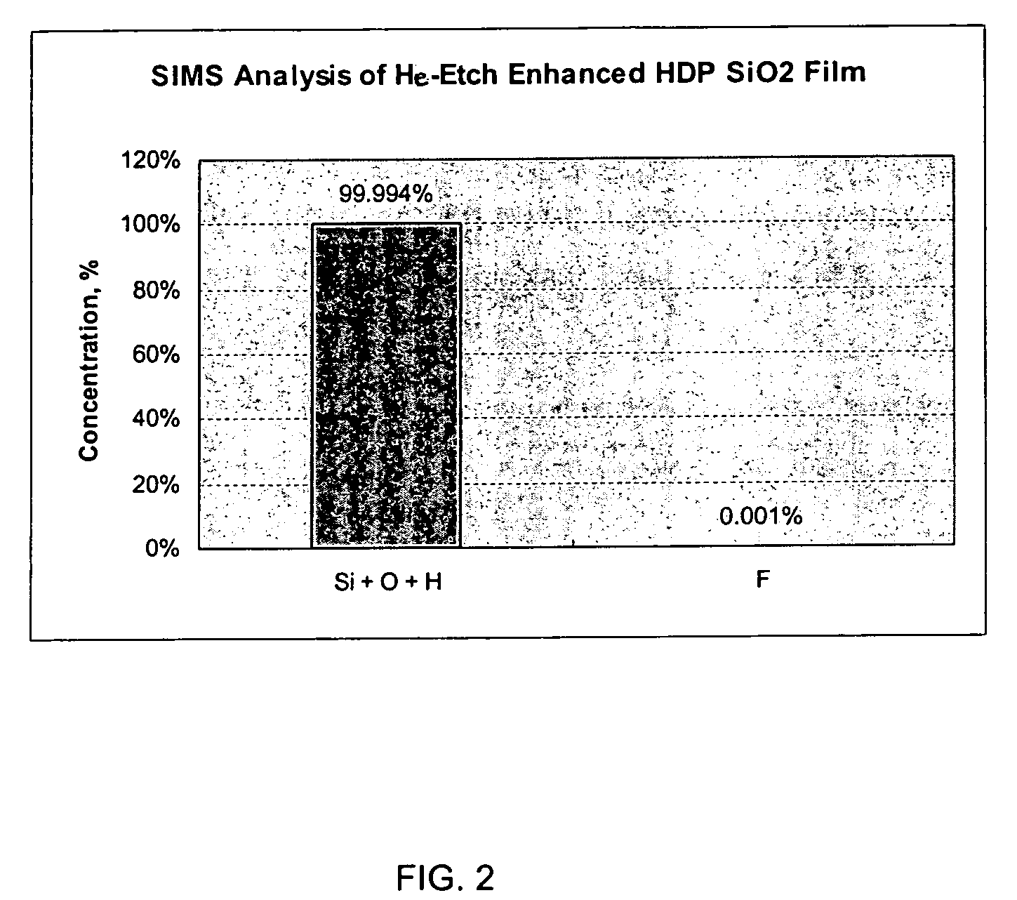
[0024]Reference will now be made in detail to specific embodiments of the invention. Examples of the specific embodiments are illustrated in the accompanying drawings. While the invention will be described in conjunction with these specific embodiments, it will be understood that it is not intended to limit the invention to such specific embodiments. On the contrary, it is intended to cover alternatives, modifications, and equivalents as may be included within the spirit and scope of the invention as defined by the appended claims. In the following description, numerous specific details are set forth in order to provide a thorough understanding of the present invention. The present invention may be practiced without some or all of these specific details. In other instances, well known process operations have not been described in detail in order not to unnecessarily obscure the present invention.

Introduction

[0025]The present invention addresses this need by providing chemical vapor ...


PUM

PropertyMeasurementUnit
aspect ratioaaaaaaaaaa
pressuresaaaaaaaaaa

Abstract

Plasma etch processes incorporating helium-based etch chemistries can remove dielectric a semiconductor applications. In particular, high density plasma chemical vapor etch-enhanced (deposition-etch-deposition) gap fill processes incorporating etch chemistries which incorporate helium as the etchant that can effectively fill high aspect ratio gaps while reducing or eliminating dielectric contamination by etchant chemical species.

Description

BACKGROUND OF THE INVENTION[0001]This invention relates to semiconductor device fabrication processes. More specifically, the invention relates to plasma-based chemical vapor deposition and etch processes for forming dielectric layers, particularly in high aspect ratio, narrow width recessed features.[0002]It is often necessary in semiconductor processing to fill high aspect ratio gaps with insulating material. This is the case for shallow trench isolation, inter-metal dielectric layers, passivation layers, etc. As device geometries shrink and thermal budgets are reduced, void-free filling of narrow width, high aspect ratio (AR) spaces (e.g., AR>3:1) becomes increasingly difficult due to limitations of existing deposition processes.[0003]The deposition of silicon dioxide (SiO2) assisted by high-density plasma chemical vapor deposition (HDP CVD)—a directional (bottom-up) CVD process—has become the preferred method for high aspect ratio gap fill. The method deposits more material a...

Claims


Application Information

Patent Timeline
Patent Type & Authority Patents(United States)
IPC IPC(8): H01L21/302H01L21/461
CPCH01L21/02164H01L21/02274H01L21/31116H01L21/31608H01L21/76837
Inventor LANG, CHI-IZHU, WENXIANLIMDULPAIBOON, RATSAMEEHUANG, JUDY H.
Owner NOVELLUS SYSTEMS
Why Eureka
Try Eureka