Solid-state imaging device

a solid-state imaging and imaging device technology, applied in the direction of radio frequency controlled devices, instruments, television systems, etc., can solve the problems of low process cost, low power consumption of mos-type image sensors, and defects in sensor cells, so as to prevent the occurrence of damage prevent the occurrence of defects in the pixel region, and prevent the occurrence of damag

Active Publication Date: 2008-03-18
138 EAST LCD ADVANCEMENTS LTD
View PDF6 Cites 13 Cited by
  • Summary
  • Abstract
  • Description
  • Claims
  • Application Information

AI Technical Summary

Benefits of technology

[0014]An advantage of the present invention is to provide a solid-state imaging device that can prevent the occurrence of damage in the pixel region by only forming a sidewall in a transistor in a peripheral region at the periphery of a pixel region.
[0015]A solid-state imaging device according to the invention includes a pixel region that have a photoelectric conversion element and a modulation part formed adjacent to the photoelectric conversion element, and a peripheral region in which a peripheral circuit including a driving circuit that drives the photoelectric conversion element and the modulation is disposed, and the peripheral region has a transistor that a sidewall is formed on a side surface of a gate electrode, and the pixel region has a transistor that a sidewall is not formed on a side surface of a gate electrode.
[0016]In such a structure, the photoelectric conversion element and the modulation are formed in the pixel region. Further, in the peripheral region, the peripheral circuit including the driving circuit that drives the photoelectric conversion element and the modulation is disposed. The peripheral region has the transistor that the sidewall is formed on the side surface of the gate electrode, and the pixel region has the transistor that the sidewall is not formed on the side surface of the gate electrode. In other words, by using the sidewall, the peripheral region obtains the transistor having an LDD structure. Meanwhile, the sidewall is not formed in the transistor in the pixel region. Accordingly, in the pixel region, etching is not performed to form the sidewall so that the substrate will not be damaged. Thus the occurrence of defects in the pixel region can be prevented.
[0017]Further, the pixel region includes: a substrate of one conductivity type; a first impurity layer of a reverse conductivity type that is formed on the substrate; a second impurity layer of one conductivity type that is formed on the first impurity layer in a forming region of the photoelectric conversion element; a third impurity layer of one conductivity type that is formed on the first impurity layer in a forming region of a transistor and to which photo generated charges are transferred from the second impurity layer; a gate electrode formed above the third impurity layer above the substrate, which gate electrode has an opening and no sidewall on a side surface thereof; a source formed on the substrate surface side in the opening, and a drain formed apart from the source and electrically coupled to the first impurity layer.
[0018]In such a structure, photo-generated charges that are generated in the first impurity layer of the photoelectric conversion element forming region are transferred from the second impurity layer to the third impurity layer. A threshold voltage of a channel of the transistor is controlled by photo-generated charges transferred to the third impurity layer, and a pixel signal corresponding to photo-generated charges is output from the transistor. The sidewall is not formed on the gate electrode that constitutes the transistor. Thus, in the pixel region, as etching is not performed to form the sidewall, the substrate is not damaged by etching. Thus the occurrence of defects can be prevented.

Problems solved by technology

The CCD type image sensor is excellent in image quality, while the CMOS type image sensor consumes lower power and its process cost is low.
But there is a problem in that defects may occur in a sensor cell due to damage in the substrate caused by performing the anisotropic etching.

Method used


Image

  • Solid-state imaging device
  • Solid-state imaging device
  • Solid-state imaging device

Examples


Embodiment Construction

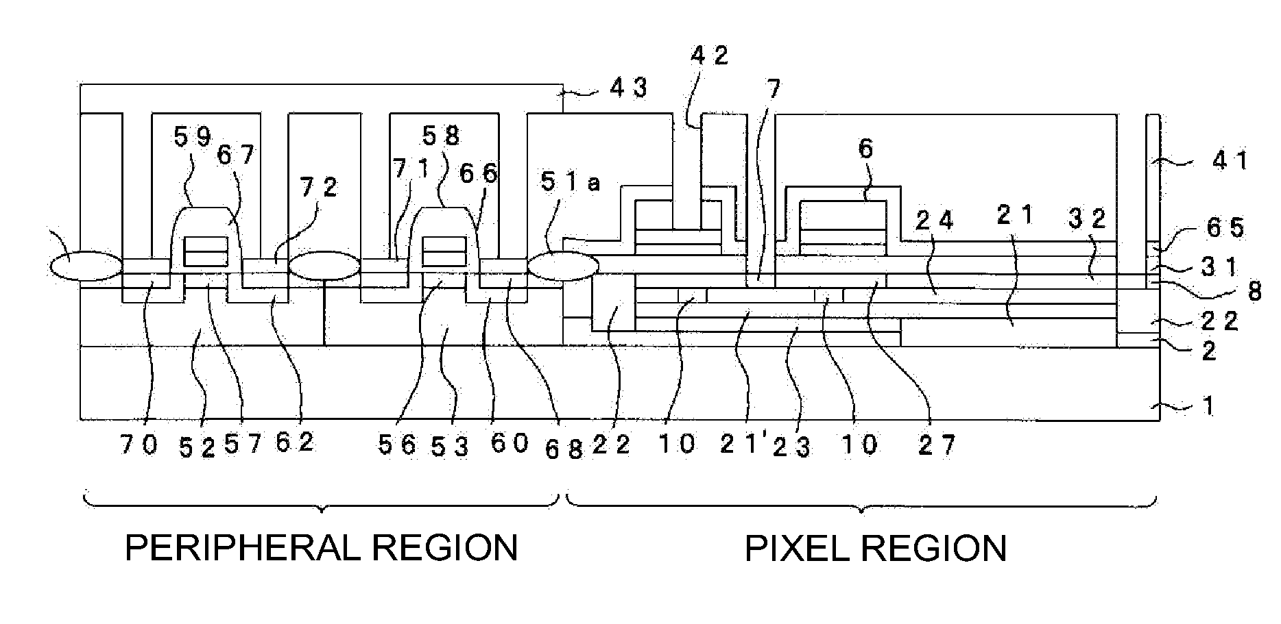
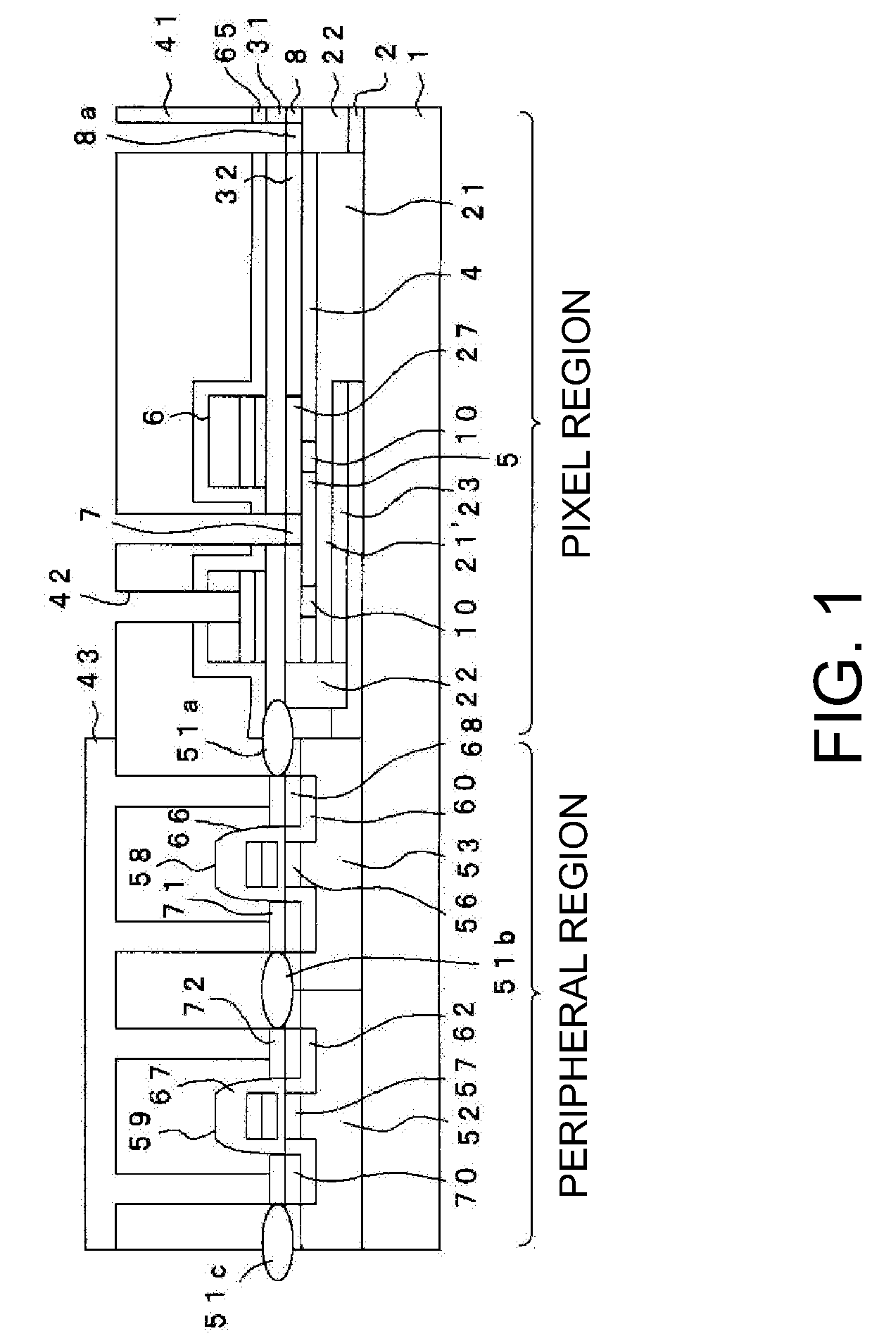
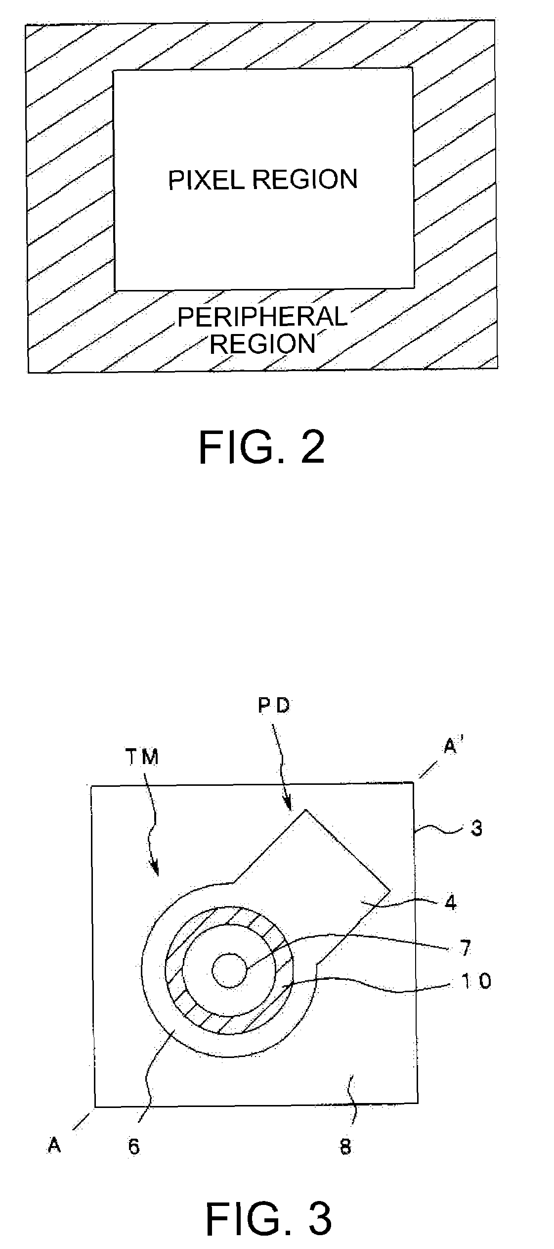
[0038]Embodiments of the present invention will now be described in detail below with reference to the drawings. FIG. 1 through FIG. 14 relate to an embodiment according to the present invention. FIG. 1 is a sectional view schematically showing a cross-section of a solid-state imaging device according to the present embodiment. FIG. 2 is an explanatory diagram illustrating a pixel region and a peripheral region of the solid-state imaging device according to the present embodiment. FIG. 3 is an explanatory diagram showing a planar shape of one sensor cell of the solid-state imaging device according to the present embodiment. Further, FIG. 1 is a sectional view showing a part of a section taken along the line A-A′ of FIG. 3. FIG. 4 is a circuit block diagram showing the entire structure of an element by an equivalent circuit. FIG. 5 through FIG. 14 are process diagrams for illustrating a method of manufacturing. Further, in the above drawings, the scale of each layer and each member a...


PUM


Abstract

A solid-state imaging device includes: a photoelectric conversion element; a pixel region including a modulation part formed adjacent to the photoelectric conversion element; and a peripheral region in which a peripheral circuit including a driving circuit driving the photoelectric conversion element and the modulation part is disposed, wherein the peripheral region includes a transistor that a sidewall is formed on a side of a gate electrode; and the pixel region includes a transistor that no sidewall is formed on a side of a gate electrode.

Description

[0001]The entire disclosure of Japanese Patent Application No. 2005-140734, filed May 13, 2005 is expressly incorporated by reference herein.BACKGROUND[0002]1. Technical Field[0003]The present invention relates to a solid-state imaging device having a high quality image and low power consumption.[0004]2. Related Art[0005]As solid-state imaging devices mounted in cellular phones and so forth, there are a charge coupled device (CCD) type image sensor and a CMOS type image sensor. The CCD type image sensor is excellent in image quality, while the CMOS type image sensor consumes lower power and its process cost is low. In recent years, MOS type solid-state imaging devices using a threshold voltage modulation method that combines both high quality image and low power consumption have been proposed. The MOS type solid-state imaging device of the threshold voltage modulation method is disclosed in Japanese Unexamined Patent Publication No. 2001-177085, for example.[0006]In an image sensor,...

Claims


Application Information

Patent Timeline
Patent Type & Authority Patents(United States)
IPC IPC(8): H01L29/04H01L27/146H04N5/335H04N5/357H04N5/369H04N5/372H04N5/374
CPCH01L27/14687H01L27/14689
Inventor SAKANO, YORITOMIZUGUCHI, AKIRANAKAMURA, NORIYUKI
Owner 138 EAST LCD ADVANCEMENTS LTD
Why Eureka
Try Eureka