Programmable embedded logic analyzer in an integrated circuit

a logic analyzer and embedded logic technology, applied in the direction of electronic circuit testing, measurement devices, instruments, etc., can solve the problems of complex integrated circuits that are often difficult to debug, problems that occur in customer environments, and the same bug that the customer experienced can be an extremely time-consuming and resource-intensive task

Inactive Publication Date: 2008-03-25
AVAGO TECH INT SALES PTE LTD
View PDF3 Cites 29 Cited by
  • Summary
  • Abstract
  • Description
  • Claims
  • Application Information

AI Technical Summary

Problems solved by technology

Complex integrated circuits are often difficult to debug, particularly in customer environments.
Problems that occur in customer environments often occur in specific configurations, environmental conditions, and instances of product.
Moreover, the customer is usually using the integrated circuit in an application optimized for production which does not contain all the usual testability interfaces that are available when the chip is production tested.
Therefore, the process of understanding the exact set-up and environment required to replicate in the chip designer's laboratory the same bug that the customer experienced can be an extremely time and resource intensive task.

Method used


Image

  • Programmable embedded logic analyzer in an integrated circuit
  • Programmable embedded logic analyzer in an integrated circuit
  • Programmable embedded logic analyzer in an integrated circuit

Examples


Embodiment Construction

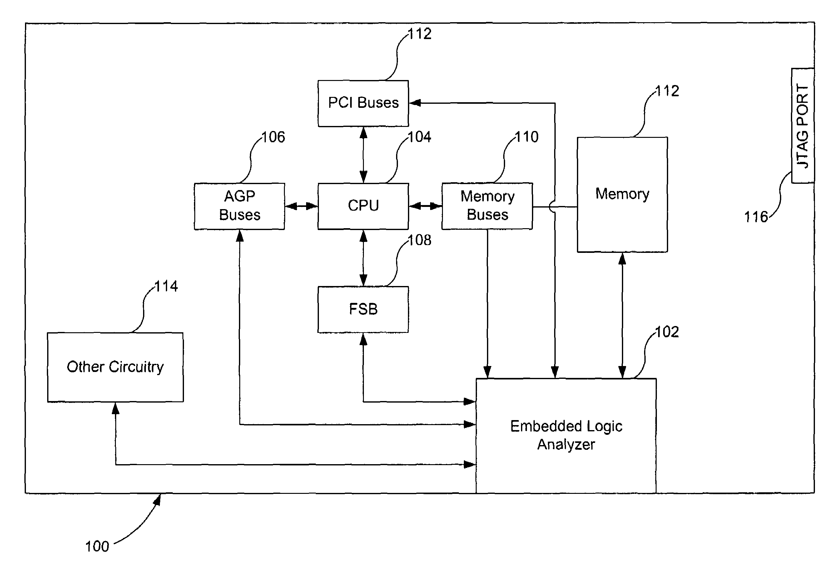
[0009]Identifying and understanding a bug in a complex chip generally requires visibility of the state and sequence of internal nodes inside the chip. These nodes are brought external to the chip via test buses. Typically, a logic analyzer is connected to these external test buses. The logic analyzer then attempts to capture the states and sequences pertinent to the creation of the bug. A special test board is then used to easily access the test bus outputs and to put the chip into a test mode.

[0010]By designing a logic analyzer function into the chip with internal access to the test buses, clocks and events of the chip, a significant improvement over previous methods of debugging problems can be achieved. The overhead in chip size needed for this function can be very small, especially if existing RAM in the design can be shared with the logic analyzer during the debug process.

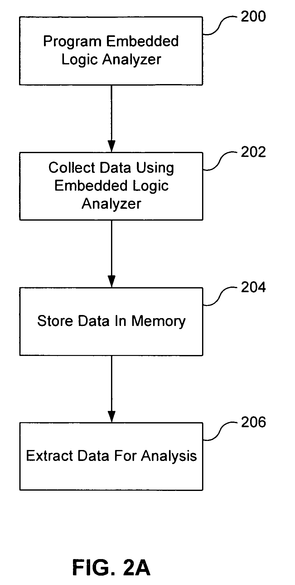
[0011]Configuration of the logic analyzer and observation of the acquired results in memory is accessed thr...


PUM


Abstract

A logic analyzer having internal access to the test buses, clocks and events of a chip is used to debug the chip. The logic analyzer is designed with the capability to share existing memory in the chip during the debug process. Additionally, the configuration of the logic analyzer and observation of the acquired results in the shared memory can be accessed through normal control interfaces of the chip and does not require special test cards. The logic analyzer includes a clocking function, a trigger function, a signal multiplexer, and a memory block. The clocking function is configured to select as the sample clock for the function any of the clocks in the integrated circuit. In addition, the clocking function may provide a means to decimate these clocks by some factor to sample over larger intervals.

Description

CROSS REFERENCE TO RELATED APPLICATIONS[0001]This application claims the benefit of U.S. Provisional Application No. 60 / 601,181 filed Aug. 13, 2004, which is incorporated herein by reference.BACKGROUND OF THE INVENTION[0002]Complex integrated circuits are often difficult to debug, particularly in customer environments. Problems that occur in customer environments often occur in specific configurations, environmental conditions, and instances of product. Moreover, the customer is usually using the integrated circuit in an application optimized for production which does not contain all the usual testability interfaces that are available when the chip is production tested. Therefore, the process of understanding the exact set-up and environment required to replicate in the chip designer's laboratory the same bug that the customer experienced can be an extremely time and resource intensive task. In addition, the customer is typically interested in identifying the root cause of the probl...

Claims


Application Information

Patent Timeline
Patent Type & Authority Patents(United States)
IPC IPC(8): G01R31/28
CPCG01R31/3177
Inventor CREIGH, JOHN LOCK
Owner AVAGO TECH INT SALES PTE LTD
Why Eureka
Try Eureka