Methods for programming a floating body nonvolatile memory

a floating body, non-volatile memory technology, applied in semiconductor devices, digital storage, instruments, etc., can solve the problems of reducing the recombination time, unable to completely or completely control the programming operation, and the inherent bipolar transistor inherent in any mos transistor becomes conductive,

Inactive Publication Date: 2008-04-01
NXP USA INC
View PDF13 Cites 27 Cited by
  • Summary
  • Abstract
  • Description
  • Claims
  • Application Information

AI Technical Summary

Problems solved by technology

As a result, if the same junction structures are used in SOI, the recombination time is very long compared to the operations (e.g. programming, reading, erasing, etc.) of the nonvolatile memory device.
Another problem is that during the programming operation the holes may build up to such an extent that they do not allow the programming operation to function completely or to fail.
Yet another problem for transistors with a floating body is that as the floating body bias becomes high, an inherent bipolar transistor inherent in any MOS transistor becomes conductive.
The biasing of the inherent transistor may result in avalanche breakdown at the drain of the floating body device.
A common symptom of this phenomena is ruptured gate oxides and thermal damage to the drain junction which permanently modifies desired electrical characteristics.
These issues limit the usefulness of implementing NVM cells on SOI.

Method used


Image

  • Methods for programming a floating body nonvolatile memory
  • Methods for programming a floating body nonvolatile memory
  • Methods for programming a floating body nonvolatile memory

Examples


Embodiment Construction

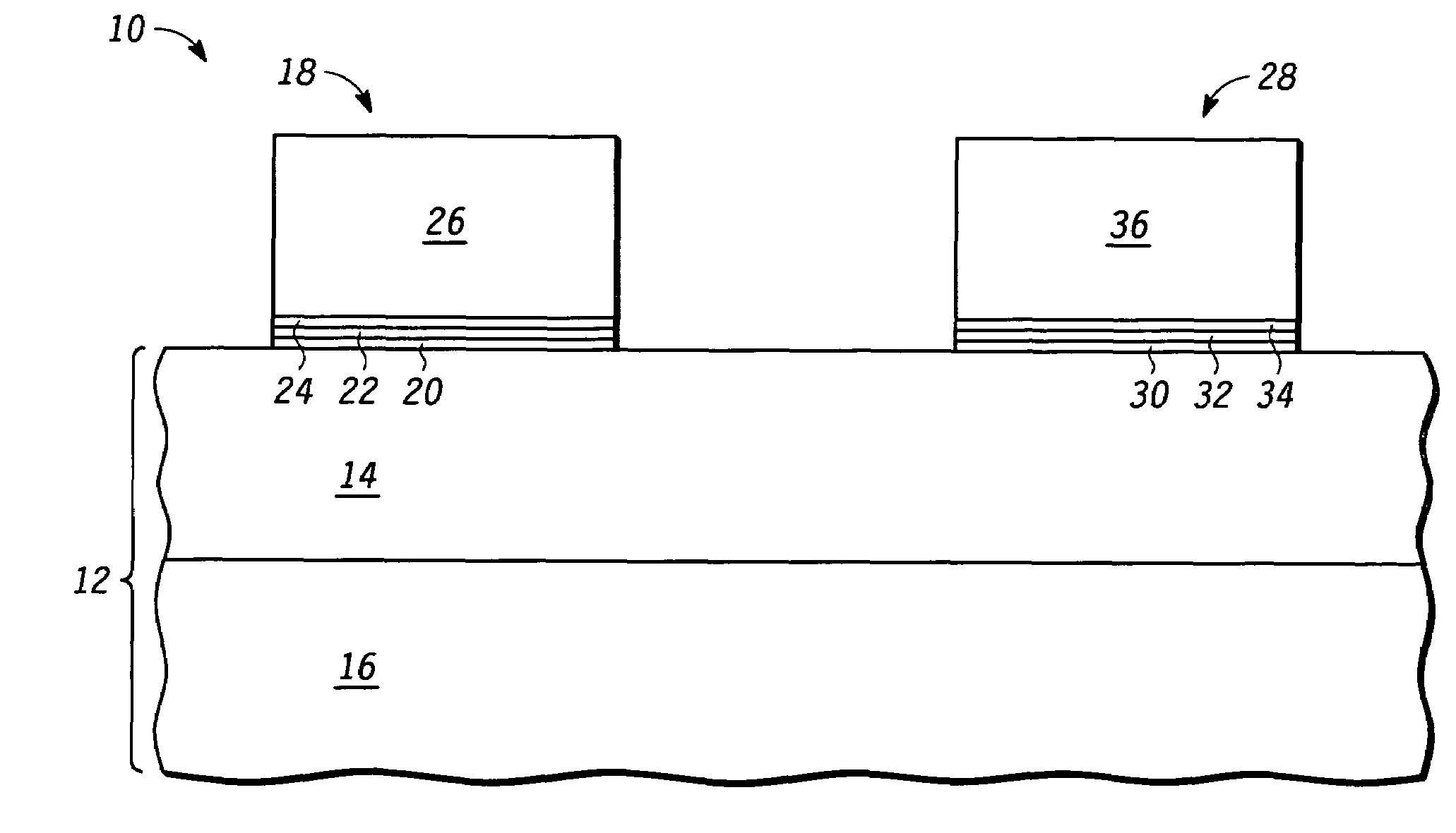
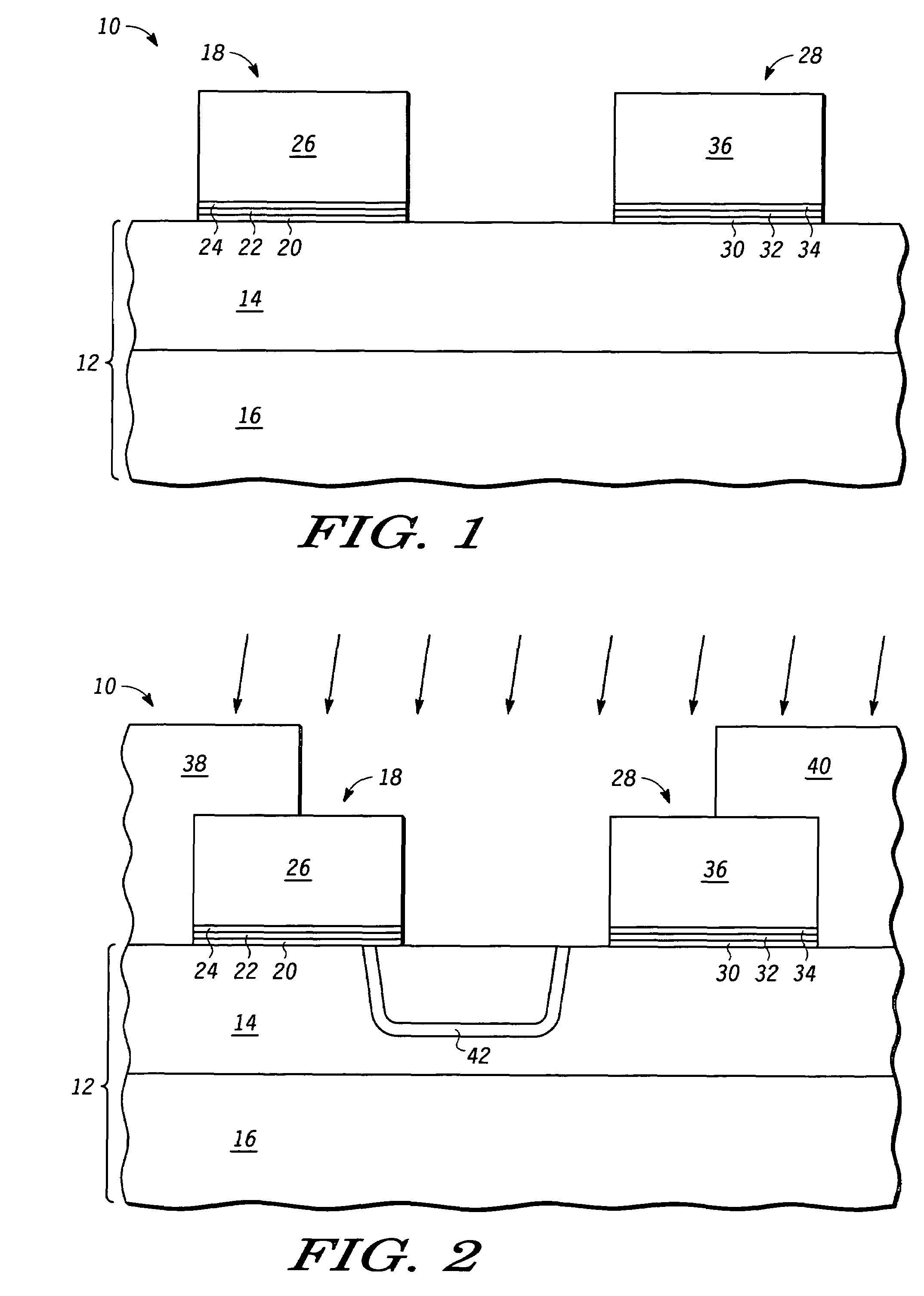
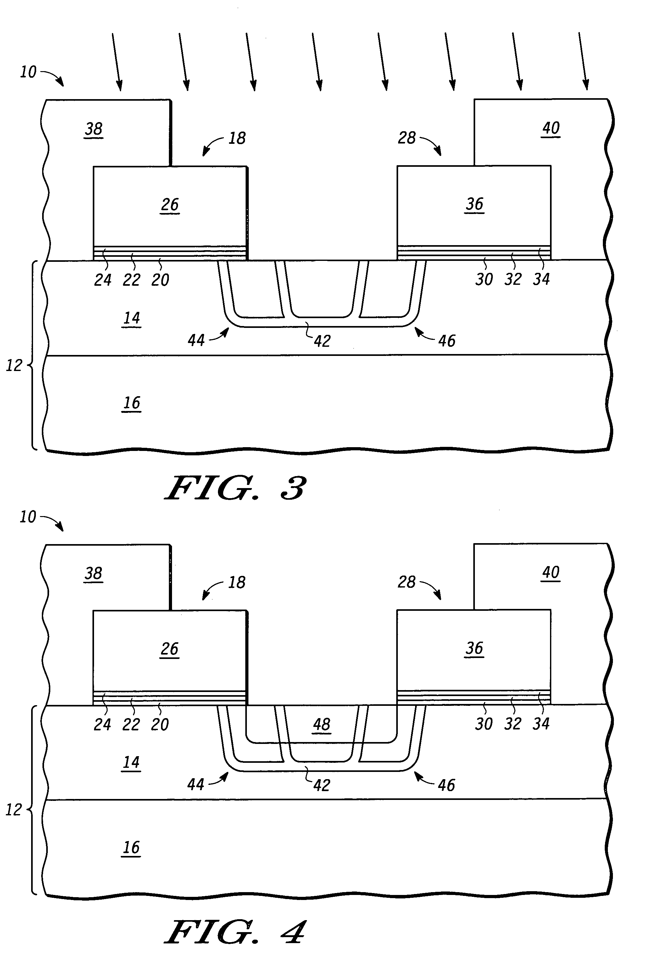
[0018]Illustrated in FIG. 1 is a semiconductor device 10 having an NVM (nonvolatile memory) cell 18 and an NVM cell 28. An insulator layer 16, commonly implemented as an oxide, is provided. Overlying the insulator layer 16 is a layer of silicon 14. Collectively, the layer of silicon 14 and insulator layer 16 is an SOI (silicon on insulator) substrate 12. In one form the layer of silicon is doped to have a P-type conductivity but it should be well understood that an opposite conductivity may be formed. NVM cell 18 has a tunnel dielectric 20 overlying the layer of silicon 14. Overlying the tunnel dielectric 20 is a charge storage layer 22. Overlying the charge storage layer 22 is a dielectric layer 24. Overlying the dielectric layer 24 is a gate 26. NVM cell 28 has a tunnel dielectric 30 overlying the layer of silicon 14. Overlying the tunnel dielectric 30 is a charge storage layer 32. Overlying the charge storage layer 32 is a dielectric layer 34. Overlying the dielectric layer 34 is...


PUM


Abstract

A technique to speed up the programming of a non-volatile memory device that has a floating body actively removes holes from the floating body that have accumulated after performing hot carrier injection (HCI). The steps of HCI and active hole removal can be alternated until the programming is complete. The active hole removal is faster than passively allowing holes to be removed, which can take milliseconds. The active hole removal can be achieved by reducing the drain voltage to a negative voltage and reducing the gate voltage as well. This results in directly withdrawing the holes from the floating body to the drain. Alternatively, reducing the drain voltage while maintaining current flow stops impact ionization while sub channel current collects the holes. Further alternatively, applying a negative gate voltage causes electrons generated by band to band tunneling and impact ionization near the drain to recombine with holes.

Description

CROSS REFERENCE TO RELATED APPLICATION[0001]This application is related to the following pending application:[0002](1) U.S. patent application Ser. No. 11 / 060,996 entitled “NVM Cell on SOI and Method of Manufacture” filed concurrently herewith and assigned to the assignee hereof.FIELD OF THE INVENTION[0003]This invention relates generally to semiconductor devices, and more specifically, to nonvolatile memory devices and methods of programming.BACKGROUND OF THE INVENTION[0004]Memory circuits are commonly manufactured using thousands of transistors to store data. Each of the transistors has a gate or control electrode and two current electrodes known as a source and a drain in metal oxide semiconductor (MOS) technology. The source and the drain typically reside in a well region formed in a substrate. The source and drain are adjacent to the gate which is commonly elevated above the source and drain. For NVM transistors, a storage layer is placed between the gate and an underlying body...

Claims


Application Information

Patent Timeline
Patent Type & Authority Patents(United States)
IPC IPC(8): G11C11/34
CPCH01L21/26586H01L27/115H01L27/11521H01L29/1083H01L29/7881H10B69/00H10B41/30
Inventor BURNETT, JAMES D.MURALIDHAR, RAMACHANDRAN
Owner NXP USA INC
Why Eureka
Try Eureka