Organic electroluminescent device and fabricating method thereof

a technology of electroluminescent devices and organic materials, applied in the manufacture of electrode systems, electric discharge tubes/lamps, electrode systems, etc., can solve the problems of increasing production costs, reducing the display size of passive matrix organic eld, and requiring a relatively high amount of power to operate, etc., to achieve the effect of simplifying the manufacturing process

Active Publication Date: 2008-04-08
LG DISPLAY CO LTD
View PDF33 Cites 28 Cited by
  • Summary
  • Abstract
  • Description
  • Claims
  • Application Information

AI Technical Summary

Benefits of technology

[0020]An advantage of the present invention is to provide an organic ELD with a simplified manufacturing process.

Problems solved by technology

While both the passive matrix organic ELD and the active matrix organic ELD have a simple structure and are formed by a simple fabricating process, the passive matrix organic ELD requires a relatively high amount of power to operate.
In addition, the display size of a passive matrix organic ELD is limited by its structure.
Therefore, production cost increases.
In addition, because the height of the separators formed of an organic material is relatively high, a metal layer that will be formed later on the organic electroluminescent layer may be undesirably cut during the deposition of the metal layer, leading to a manufacturing defect.
Moreover, the organic material dispensed in the pixel regions by an inkjet method is not uniform.

Method used


Image

  • Organic electroluminescent device and fabricating method thereof
  • Organic electroluminescent device and fabricating method thereof
  • Organic electroluminescent device and fabricating method thereof

Examples


first embodiment

[0052]FIGS. 6A to 6E are schematic cross-sectional views illustrating a fabricating process according to present invention.

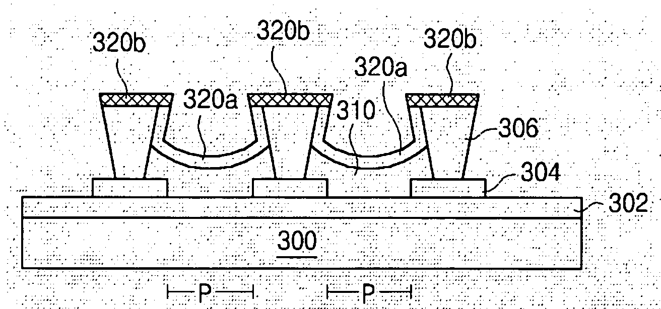
[0053]In FIG. 6A, pixel regions “P” is defined in a substrate 300. A first electrode 302 is formed on the substrate 300 including the pixel regions “P.” The first electrode 302 is made of a transparent conductive material such as tin oxide (ITO), indium zinc oxide (IZO), indium tin zinc oxide (ITZO), or the like. Then, an insulating layer 304 is formed on the first electrode 302 at boundaries of the pixel regions “P” to prevent shorting between the first electrode 302 and a second electrode that will be formed later. Although not shown in FIG. 6A, the insulating layer 304 may be formed as one body in a plan view. In addition, the insulating layer 304 may be formed by depositing and patterning silicon nitride (SiNx) or silicon oxide (SiO2), or by coating and patterning polyimide. For example, a process for patterning a polyimide layer may be a photolithography pr...

second embodiment

[0059]FIGS. 7A to 7G are schematic cross-sectional views illustrating a fabricating process according to present invention.

[0060]In FIG. 7A, pixel regions “P” is defined in a substrate 400. A first electrode 402 is formed on the substrate 400 including the pixel regions “P.” The first electrode 402 is made of a transparent conductive material such as tin oxide (ITO), indium zinc oxide (IZO) and indium tin zinc oxide (ITZO), or the like. Then, an insulating layer 404a is formed on the first electrode 402 at boundaries of the pixel regions “P” to prevent shorting between the first electrode 402 and second electrodes that will be formed later. Although not shown in FIG. 7A, the insulating layer 404a may be formed as one body in a plan view. In addition, the insulating layer 404a may be formed by depositing and patterning silicon nitride (SiNx) or silicon oxide (SiO2), or by coating and patterning polyimide. For example, the patterning step may include a photolithography process using a...

third embodiment

[0071]FIGS. 8A to 8E are schematic cross-sectional views illustrating a fabrication process according to present invention.

[0072]In FIG. 8A, pixel regions “P” is defined in a substrate 500. A first electrode 502 is formed on the substrate 500 including the pixel regions “P.” The first electrode 502 is made of a transparent conductive material such as indium tin oxide (ITO), indium zinc oxide (IZO), indium tin zinc oxide (ITZO), or the like. Then, an insulating layer 504 is formed on the first electrode 502 at boundaries of the pixel regions “P” to prevent shorting between the first electrode 502 and a second electrode that will be formed later. Although not shown in FIG. 8A, the insulating layer 504 may be formed as one body as observed in a plan view. In addition, the insulating layer 504 may be formed by depositing and patterning silicon nitride (SiNx) or silicon oxide (SiO2), or the insulating layer may be formed by coating and patterning polyimide. For example, a the patterning ...


PUM

PropertyMeasurementUnit
timeaaaaaaaaaa
temperatureaaaaaaaaaa
electroluminescentaaaaaaaaaa

Abstract

A method of fabricating a substrate for an organic electroluminescent device includes forming a first electrode on a substrate having a pixel region; forming an insulating layer on the first electrode at a boundary of the pixel region; forming an electroluminescent layer on the first electrode in the pixel region by printing a solution type electroluminescent material; forming a second electrode material layer on an entire surface of the substrate having the electroluminescent layer and the insulating layer; and oxidizing or ablating by laser the second electrode material layer at the boundary of the pixel region to form a second electrode in the pixel region and a metal oxide layer at the boundary of the pixel region.

Description

[0001]The present invention claims the benefit of the Korean Patent Application No. 2003-100676 filed in Korea on Dec. 30, 2003, which is hereby incorporated by reference for all purposes as if fully set forth herein.BACKGROUND OF THE INVENTION[0002]1. Field of the Invention[0003]The present invention relates to an organic electroluminescent device (ELD), and more particularly to a dual plate type organic ELD and a method of fabrication thereof.[0004]2. Discussion of the Related Art[0005]In general, an organic ELD emits light by injecting electrons from a cathode and holes from an anode into a luminescence layer, combining the electrons with the holes, generating excitons, and transitioning the excitons from an excited state to a ground state. Compared to a liquid crystal display (LCD) device, an additional light source is not necessary for the organic ELD to emit light because the transition of the excitons between the two states causes light to be emitted. Accordingly, the size an...

Claims


Application Information

Patent Timeline
Patent Type & Authority Patents(United States)
IPC IPC(8): H01J9/24H05B33/26H05B33/22H01L27/32H01L51/00H01L51/52H01L51/56H05B33/10
CPCH01L27/3246H01L51/0005H01L51/5203H01L27/3251H01L51/5221H01L51/56H10K59/127H10K71/135H10K59/122H10K50/82H10K71/00H10K59/805H05B33/22H10K50/805
Inventor LEE, JAE-YOON
Owner LG DISPLAY CO LTD
Why Eureka
Try Eureka